• Opto-Electronic Advances
  • Vol. 4, Issue 9, 200064-1 (2021)
Wei Liu, Zhuxin Li, Zengliang Shi, Ru Wang, Yizhi Zhu, and Chunxiang Xu*
Author Affiliations
  • State Key Laboratory of Bioelectronics, School of Biological Sciences & Medical Engineering, Southeast University, Nanjing 210096, China
  • show less
    DOI: 10.29026/oea.2021.200064 Cite this Article
    Wei Liu, Zhuxin Li, Zengliang Shi, Ru Wang, Yizhi Zhu, Chunxiang Xu. Nano-buffer controlled electron tunneling to regulate heterojunctional interface emission[J]. Opto-Electronic Advances, 2021, 4(9): 200064-1 Copy Citation Text show less

    Abstract

    Interface emission from heterojunction is a shortcoming for electroluminescent devices. A buffer layer introduced in the heterojunctional interfaces is a potential solution for the challenge. However, the dynamics for carrier tunneling to control the interface emission is still a mystery. Herein, the low-refractive HfO2 with a proper energy band configuration is employed as the buffer layer in achieving ZnO-microwire/HfO2/GaN heterojunctional light-emitting diodes (LEDs). The optically pumped lasing threshold and lifetime of the ZnO microwire are reduced with the introduced HfO2 layer. As a result, the interface emission is of blue-shift from visible wavelengths to 394 nm whereas the ultraviolet (UV) emission is enhanced. To regulate the interface recombination between electrons in the conduction band of ZnO and holes in the valence band of GaN, the tunneling electrons with higher conduction band are employed to produce a higher tunneling current through regulation of thin HfO2 film causing blue shift and interface emission enhancement. Our results provide a method to control the tunneling electrons in heterojunction for high-performance LEDs.

    Introduction

    The heterojunction is one of the approaches to construct functional devices in semiconductors that are difficult to implant both n- and p-type conduction. However, undesired emission (interface emission) from electroluminescence (EL) usually happens at the interface due to the mismatched energy band configuration. Generally, a proper buffer layer was introduced to suppress the interface emission and improve the intrinsic emission1. In this case, the devices have to work at a higher turn-on voltage with higher energy consumption. Furthermore, the bottle-neck of p-doped ZnO has seriously impeded its desired application in short-wavelength optoelectronics2, especially as ultraviolet (UV) laser diodes3. Therefore, ZnO/GaN heterojunctions have been designed and the various layers have been introduced as the electron barrier layers, such as Ga2O34, ZnS5, MgO6, 7, Al1-xGaxN3, AlN8, 9, HfO210, MgF11, Al2O312, NiO13 and In0.17Al0.83N14. In these reports, the turn-on voltages have been elevated by increasing the thickness of electron barrier layers. It is expected to suppress the interface emission through insertion of a proper buffer layer with certain thickness (≥ 20 nm) for controlling the tunneling electrons or holes12, 13, 15. In these situations, the UV emission of p-type GaN16, 17 and interface emission were both reduced. However, is it possible to take advantage of the interface emission? How to control and utilize the interface emission still needs to be studied in the heterojunctional display field.

    For the case of ZnO/GaN, another issue is the inevitable optical loss at the interface due to the similar refractive index of GaN and ZnO18. The insertion of buffer layer with a low refractive index is an effective way to improve the UV emission. For example, Zhu et al.18 introduced a PVK layer between ZnO micro-rod and GaN substrate and confined the optical field in ZnO cavity effectively. This was a prominent method to reduce optical loss and improve EL via insertion of a proper buffer layer.

    In this work, a thin HfO2 film was introduced between ZnO and GaN to improve light reflectivity of interface and regulate tunneling electrons in the heterojunction. The influences of the thin HfO2 film on PL of ZnO microwire (MW) as well as EL of ZnO MW/HfO2/GaN light-emitting diodes (LEDs) were studied experimentally and theoretically. It was found that the improved UV emission of device with blue-shifted interface emission increased from 66.26% to 76.14% using HfO2 with the optimized thickness of 5 nm. Moreover, the optical gain and loss were evaluated through whispering-gallery mode (WGM) lasing. Moreover, the electron tunneling dynamics was discussed based on the energy band configuration.

    Experiment

    Material synthesis and device fabrication

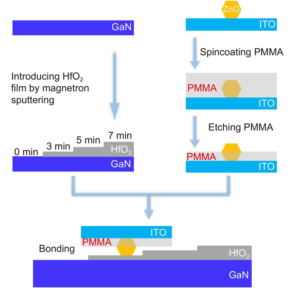
    The n-type ZnO MWs were synthesized by using a chemical vapor deposition (CVD) method in our previous work19. To systematically study the buffer influence on the EL of the device, the HfO2 film was deposited on the GaN film by radio frequency magnetron sputtering with an HfO2 target (99.99%). By moving the masks and changing the time of magnetron sputtering (3, 5, and 7 min), a stepped HfO2 film was fabricated, and each step was named GaN 1, GaN 2, GaN 3 and GaN 4 respectively, as shown Fig. 1. The diagram of device fabrication is shown in Fig. 1. The individual ZnO MWs were placed on the steps for in-situ µ-PL analysis, and then were bonded with ITO and GaN films to form ITO/ZnO/HfO2/GaN LEDs separated by PMMA. Finally, the ITO/ZnO/HfO2/GaN LEDs constructed by ITO bonded ZnO MW are named as LED 1, LED 2, LED 3, and LED 4, respectively.

    The diagram of device fabrication.

    Figure 1.The diagram of device fabrication.

    Instruments

    The atomic force microscope (AFM) images were measured in tapping mode by Brukers Dimension Icon Atomic Force Microscopy under ambient conditions. Optically pumped spectra of the device were measured by a home-made confocal microphotoluminescence (µ-PL) setup (Olympus BX35) excited by a 325 nm femtosecond pulsed laser with a 10× objective. The EL and I-V characteristics of the samples were conducted in a cooling-heating stage (INSTEC mk2000), with the µ-PL setup and a semiconductor characterization system (Keithley 4200). The PL and EL spectra were all collected through a spectrometer (Princeton Instruments Acton SP2500i). Time-resolved PL (TR-PL) was measured by a streak camera (Optronis Optoscope sc-10) and a femtosecond pulsed laser (100 fs pulsed duration and 1 kHz repetition rate) as signal detector and excitation source, respectively.

    Simulations

    The proposed structure is analyzed using a finite element method (FEM). The reflectivity of interface in these structures is simulated. In the simulation, the refractive indices of the ZnO, HfO2 and GaN were taken to be 2.5, 1.98 and 2.3, respectively. The thicknesses of the ZnO layer and GaN layer were both set to be 2.5 μm. The HfO2 layer was inserted between the ZnO layer and GaN layer, where the thicknesses were 0, 5.03, 8.79 and 12.55 nm. The light is perpendicularly emitted from the ZnO at the wavelength of 390 nm.

    Quantum size effects are not significant in the ZnO MW, so a 1D semi-empirical method can be used in the simulation. As displayed on the inset of Fig. 7(b), the thickness of the device was 1 μm with an n-type doping concentration of 1 × 1016 cm−3 for ZnO and a p-type doping concentration of 1 × 1017 cm−3 for GaN, in which the thickness of insulating layer was adjustable. The driving voltage was 40 V. To illustrate the basic physics simply, the electrodes at the ends of the device were assumed to be Ohmic contacts and the Dirichlet boundary conditions were applied for the carrier concentration and electrical potential. The thermionic emission model to determine the current transfer occurring between the different materials and Shockley-Read-Hall recombination feature were considered as well. The distributions of conduction band and valence band were analyzed near the ZnO-HfO2-GaN junctions, which is modulated by the thickness of HfO2.

    Results and discussion

    The schematic diagram and EL spectra for ZnO/GaN LED are shown in Fig. 2(a) and 2(b), respectively. Moreover, the peak of PL spectra for ZnO MW and GaN film at 391 nm and 379 nm are demonstrated in the inset of Fig. 2(b). The EL spectrum of ZnO/GaN LED includes three parts: peaks at 379 nm from GaN, 391 nm from ZnO and 414 nm from the interface emission, respectively. The HfO2 film was tested by a stepped structure shown in Fig. 3(a) using AFM. The thickness of the HfO2 film in GaN 2 is 5.03 nm, GaN 3 is 8.79 nm and GaN 4 is 12.55 nm as shown in Fig. 2(c)2(f). The AFM image of GaN film in Fig. 2(g) exhibits a smooth surface with the average roughness of ~0.551 nm. The morphology of GaN film became smoother with the average roughness of ~0.337 nm after the modification by HfO2, as shown in Fig. 2(h). It can be observed that the interface contact can be improved after the GaN film bonded with HfO2.

    (a) A schematic diagram for ZnO/GaN LEDs. (b) The Gaussian decomposition of EL spectra for LED and the inset depicts the PL spectra of the GaN film as well as ZnO MWs. (c−f) The height of the step-like HfO2 film with different sputtering time (c) 2 min, (d) 3 min, (e) 5 min and (f) 7 min. (g, h) AFM image for the GaN surface (g) before and (h) after bonding HfO2 film with thickness of 5.03 nm.

    Figure 2.(a) A schematic diagram for ZnO/GaN LEDs. (b) The Gaussian decomposition of EL spectra for LED and the inset depicts the PL spectra of the GaN film as well as ZnO MWs. (c−f) The height of the step-like HfO2 film with different sputtering time (c) 2 min, (d) 3 min, (e) 5 min and (f) 7 min. (g, h) AFM image for the GaN surface (g) before and (h) after bonding HfO2 film with thickness of 5.03 nm.

    (a) Schematic diagram of ZnO/HfO2/GaN for in-situ optical test. (b) Lasing emission intensity for ZnO MW versus the excitation power density on different substrates. (c−f) the corresponding PL spectra under different excitation power densities for ZnO MW with different thickness of HfO2 films: (c) 0 nm, (d) 5.03 nm, (e) 8.79 nm and (f) 12.55 nm.

    Figure 3.(a) Schematic diagram of ZnO/HfO2/GaN for in-situ optical test. (b) Lasing emission intensity for ZnO MW versus the excitation power density on different substrates. (cf) the corresponding PL spectra under different excitation power densities for ZnO MW with different thickness of HfO2 films: (c) 0 nm, (d) 5.03 nm, (e) 8.79 nm and (f) 12.55 nm.

    In order to investigate the influence of HfO2 thickness on optical gain and loss of ZnO MW/HfO2/GaN heterjunctions, the in-situ PL experiments were carried out and the obtained lasing spectra for ZnO MW on GaN films with different excitation power densities are displayed in Fig. 3. All samples demonstrated the WGM behaviors and the lasing characteristics, i.e., lasing threshold, intensity, and position, are modulated depending on the variations in the modified film at the boundaries of the cavity.

    Although the lasing modes were located at the same position, the number of modes is increased from 9 to 11 at the same excitation power of 20.4 μW, as shown in Fig. 3(c) and 3(d). In addition, the lasing was enhanced at the same excitation power and lasing thresholds of ZnO MW on GaN 2, 3 and 4 were lower than that of GaN 1 as shown in Fig. 3(b). In order to understand the reason, the reflectivity at 390 nm was simulated by a multi-physical field method. It can be seen that the reflectivity of 390 nm was increased (0.129, 0.132, 0.140, 0.153 and 0.283) with the film thickness increasing. The thresholds of ZnO-MW lasing were decreased whereas the quality of microcavity is increased by the HfO2 modified GaN film.

    For more insights into dynamic coupling processes, the time-resolved photoluminescence (TRPL) spectra were recorded at room temperature, as shown in Fig. 4. The normalized TRPL decay curves of the ZnO MW on GaN 1, GaN 2, GaN 3, and GaN 4 (the detailed definition is in Experiment part) were well-fitted by the mono-exponential function. The decay lifetime19-21 is defined as follows:

    The lifetime of ZnO MW on various substrates with excitation power of 8 μW.

    Figure 4.The lifetime of ZnO MW on various substrates with excitation power of 8 μW.

    $ I(t) = {I_0}{\rm{exp}} \left( { - t/{\tau _{{{{\rm{photonic}} }}}}} \right)\;, $ ()

    here, I0 is the starting PL intensity before the decay. The reduction for the lifetime of ZnO MW from 113 ps to 89 ps after bonding the HfO2 film is attributed to the aggravation of non-radiative transition. The PL intensity of ZnO MW was therefore enhanced after the HfO2 film modification, which is in agreement with the results of in-suit PL experiments as depicted in Fig. 3. Due to the inserted HfO2 buffer layer with low refractive index, the reflectivity of GaN film was increased to improve the Q factor of the ZnO MW microcavity. The laser threshold was hence decreased by the increasing of the thickness of the HfO2 film. After the interface was modified by the HfO2 film, the reflectivity was enhanced and roughness was reduced. The Purcell effect is therefore strengthened.

    A schematic diagram of ZnO/HfO2/GaN LED and I-V curves of these LEDs are depicted in Fig. 5(a). After the HfO2 film was sputtered on the interface of the GaN film, the I-V curve of the devices displayed a better rectification property. The turn-on voltage was increased with the HfO2 film thickening. Although the driving voltage increases to 40 V, the device with 60 nm HfO2 film still had no current produced (Open circuit state). The normalized EL spectra of the LEDs under a driving current of 1 mA are shown in Fig. 5(b). It was observed that the blue shift of the EL spectra occurred after 5.03 nm HfO2 film bonding. Meanwhile, the spectrum of the device was the bluest in chromaticity coordinates (CIE 1931) in Fig. 5(g). The EL spectra and light pictures of the devices are shown in Fig. 5(c)-5(f). The light picture shows a same bluish violet after HfO2 film bonding. The device with 5.03-nm-thick HfO2 film had the highest brightness light emission under the same current as shown in Fig. 5(h). It was attributed to high electron tunneling efficiency of the device with 5.03 nm HfO2 film and the Q-factor enhancement on the microcavity of ZnO MW. It should be noted that the devices with HfO2 films (more than 5.03 nm) had the lower brightness than that of the device without HfO2 film at the same current. It was attributed to the fact that more electrons were lost non-radiatively during the electron tunneling process in the thicker HfO2 film.

    (a) I-V characteristics of ITO/ZnO/HfO2/GaN LEDs. The inset is a schematic diagram for ITO/ZnO/HfO2/GaN LEDs. (b) Normalized EL spectra for LEDs under an excitation current of 1 mA. (c−f) EL intensity of ZnO/HfO2/GaN LEDs with HfO2 films of different thickness and the inset is the light pictures: (c) 0 nm, (d) 5.03 nm, (e) 8.79 nm, (f) 12.55 nm. (g) Chromaticity coordinates of the spectra in (b). (h) EL peak intensities of the LEDs from (c) to (f).

    Figure 5.(a) I-V characteristics of ITO/ZnO/HfO2/GaN LEDs. The inset is a schematic diagram for ITO/ZnO/HfO2/GaN LEDs. (b) Normalized EL spectra for LEDs under an excitation current of 1 mA. (c−f) EL intensity of ZnO/HfO2/GaN LEDs with HfO2 films of different thickness and the inset is the light pictures: (c) 0 nm, (d) 5.03 nm, (e) 8.79 nm, (f) 12.55 nm. (g) Chromaticity coordinates of the spectra in (b). (h) EL peak intensities of the LEDs from (c) to (f).

    In order to understand the change in origin of EL spectrum of the device, the EL of devices at the current of 1 mA was analyzed by a Gaussian method as shown in Fig. 6(a−d). The EL spectra of LEDs demonstrated three peaks which were centered at ~379 nm, ~390 nm and ~410 nm, respectively. In Fig. 6(a)6(d), it can be observed that the Gaussian curves fitted well with the experimental curves. In consideration of the PL spectra for GaN with ZnO, the UV emission bands were centered at 379 nm and 390 nm related to near-band-edge recombination of GaN and ZnO, whereas the emission band at ~410 nm was corresponding to the recombination of tunneling electrons in ZnO and the holes in GaN1, 22. The location of EL emission peak of the recombination in GaN and ZnO was varied slightly with the change of the thickness of HfO2 film, while the interface emission by the recombination of tunneling electrons of ZnO and holes in GaN was located from 394 nm to 416 nm, respectively. For LED 1, LED 2, LED 3 and LED 4, the emission peaks were located at ~412 nm, ~394 nm, ~416 nm and ~414 nm. To understand the UV content of the devices, the integral intensities of UV (<400 nm) and visible spectra (> 400 nm and < 700 nm) were calculated as shown inFig. 6(a)6(d). From the insets of Fig. 6(a)6(d), it can be observed that the UV light content of LED 1, LED 2, LED 3, and LED 4 are 66.26%, 76.14%, 61.30% and 58.61%, respectively. Interestingly, LED 2 has high-content UV light emission with high brightness. The peak positions and full width at half maxima (FWHM) of emissions are displayed in Fig. 6(e) and 6(f). All the emission peak positions are blue shifted. Especially, the interface emission is become narrow and blue shifted from 414 nm to 394 nm after introducing the 5.03 nm HfO2 film.

    Gaussian conversion of Fig. 5(c)−5(f) at a current of 1 mA: (a) 0 nm, (b) 5.03 nm, (c) 8.79 nm, (d) 12.55 nm, and the inset images depict the contents of UV and visible lights. (e) The peak positions of emissions and (f) FWHM of emissions for these LEDs.

    Figure 6.Gaussian conversion of Fig. 5(c)−5(f) at a current of 1 mA: (a) 0 nm, (b) 5.03 nm, (c) 8.79 nm, (d) 12.55 nm, and the inset images depict the contents of UV and visible lights. (e) The peak positions of emissions and (f) FWHM of emissions for these LEDs.

    The p-type GaN in our work had a strong UV emission peak at 379 nm as shown in Fig. 6(a) to 6(d), which is well matched with the previous reports16, 17. The hole carrier concentration of GaN film is 3.0 × 1017 cm−3. The PL spectrum shown in Fig. 2(b) was in agreement with the results of EL spectra of GaN and ZnO in the LEDs. The energy level position changes of interface on the junction were influenced by the thickness of HfO2 film as simulated in Fig. 7(a). Serious band bending phenomenon occurred after introducing HfO2 buffer layer indicating higher level tunneling electron-hole recombination after bonding HfO2 film. When the thickness of buffer layer was increased, the band bending became smooth, resulting in blue shift from recombination between tunneling electrons of ZnO and holes of GaN after bonding thin HfO2 film. To systematically investigate the migration of electron in heterojunction, the distributions of electronic current influenced by different thicknesses of HfO2 film were simulated using the finite element method. The results are shown in Fig. 7(b) with a band structure diagram. The electrons were gathered at the highest electronic current density and formed the tunneling current of the device with the 5.03 nm HfO2 film.

    (a) Energy band of ZnO/HfO2/GaN LEDs based on theoretical simulation. (b) The distribution of electronical current density in ZnO/HfO2/GaN LEDs. The inset picture displays a structure diagram of simulation.

    Figure 7.(a) Energy band of ZnO/HfO2/GaN LEDs based on theoretical simulation. (b) The distribution of electronical current density in ZnO/HfO2/GaN LEDs. The inset picture displays a structure diagram of simulation.

    Schematic band structures based on theoretical simulation of transportations of the electrons and holes in these structures are illustrated in Fig. 8(a)8(c). Different from previous reports10, the electrons in these devices with different thicknesses of HfO2 films tunneled through HfO2 film in the junction as shown in Fig. 8(b) and 8(c). In Fig. 8(b), it can be observed that the electrons tunneled through the thin HfO2 film (5.03 nm) and a part of electrons produced in ZnO was gathered at higher conduction band. Then they tunneled into valence band of GaN based on theoretical simulation as shown in Fig. 8(b). This was the reason for the blue shift (394 nm) at the interface between ZnO and GaN. From Fig. 8(c), it was noted that the electrons were difficult to tunnel through the thick HfO2 film and only a small part of electrons tunneled into valence band of GaN because of energy losses. The main reason was the recombination at the interface between ZnO and GaN with a red shift (414 nm) after a bonding of thicker HfO2 film. The device modified with the thin HfO2 film regulated the interface emission from visible to ultraviolet through controlling the electron tunneling process and produced a higher brightness UV light.

    Schematic band structures of (a) ZnO/GaN, (b) ZnO /thin HfO2/ GaN and (c) ZnO /thick HfO2/ GaN.

    Figure 8.Schematic band structures of (a) ZnO/GaN, (b) ZnO /thin HfO2/ GaN and (c) ZnO /thick HfO2/ GaN.

    Conclusions

    In summary, ZnO/HfO2/GaN UV LEDs were fabricated, and the tunneling electrons as well as optical losses in the LED were regulated though a nano HfO2 layer. The PL spectra of ZnO MW were enhanced and threshold of the laser was decreased (from 19.8 μW to 16.7 μW) at the same time based on in-situ PL experiment. Considering the device, the tunneling electrons with higher conduction band produced a higher tunneling current which is regulated by the thin HfO2 film. As a result, the peak position of interface emission by the recombination of the tunneling electrons in ZnO and holes in GaN had a blue shift (from 414 nm to 394 nm) with increment in content of UV light (<400 nm) (from 66.26% to 76.14%). Over all, the interface emission of LED was regulated from visible to ultraviolet via insertion of a thin HfO2 buffer layer. The method provided a way to improve the performance of UV LEDs and regulate the tunneling electrons in heterojunction for illumination, display, and medical fields.

    References

    [1] DT You, CX Xu, FF Qin, Z Zhu, AG Manohari et al. Interface control for pure ultraviolet electroluminescence from Nano-ZnO-based heterojunction devices. Sci Bull, 63, 38-45(2018).

    [2] JZ Wu, H Long, XL Shi, S Luo, ZH Chen et al. Polariton lasing in InGaN quantum wells at room temperature. Opto-Electron Adv, 2, 190014(2019).

    [3] ARK Kalapala, D Liu, SJ Cho, JP Park, DY Zhao et al. Optically pumpedS room temperature low threshold deep UV lasers grown on native AlN substrates. Opto-Electron Adv, 3, 190025(2020).

    [4] LC Zhang, FZ Zhao, FF Wang, QS Li. Improvement in electroluminescence performance of n-ZnO/Ga2O3/p-GaN heterojunction light-emitting diodes. Chin Phys B, 22, 128502(2013).

    [5] LC Zhang, QS Li, L Shang, FF Wang, C Qu et al. Improvement of UV electroluminescence of n-ZnO/p-GaN heterojunction LED by ZnS interlayer. Opt Express, 21, 16578-16583(2013).

    [6] LC Zhang, QS Li, L Shang, ZJ Zhang, RZ Huang et al. Electroluminescence from n-ZnO: Ga/p-GaN heterojunction light-emitting diodes with different interfacial layers. J Phys D: Appl Phys, 45, 485103(2012).

    [7] GY Zhu, JT Li, ZL Shi, Y Lin, GF Chen et al. Ultraviolet electroluminescence from n-ZnO/i-MgO/p+-GaN heterojunction light-emitting diodes fabricated by RF-magnetron sputtering. Appl Phys B, 109, 195-199(2012).

    [8] JB You, XW Zhang, SG Zhang, JX Wang, ZG Yin et al. Improved electroluminescence from n-ZnO/AlN/p-GaN heterojunction light-emitting diodes. Appl Phys Lett, 96, 201102(2010).

    [9] SG Zhang, XW Zhang, ZG Yin, JX Wang, JG Dong et al. Improvement of electroluminescent performance of n-ZnO/AlN/p-GaN light-emitting diodes by optimizing the AlN barrier layer. J Appl Phys, 109, 093708(2011).

    [10] HH Huang, GJ Fang, XM Mo, H Long, LY Yuan et al. ZnO-based fairly pure ultraviolet light-emitting diodes with a low operation voltage. IEEE Electron Device Lett, 30, 1063-1065(2009).

    [11] S Jeong, H Kim. High light output efficiency of n-ZnO/p-GaN heterojunction light-emitting diodes fabricated with a MgF2 electron-blocking layer. Appl Phys Express, 9, 015501(2016).

    [12] L Yang, WZ Liu, HY Xu, JG Ma, C Zhang et al. Enhanced near-UV electroluminescence from p-GaN/i-Al2O3/n-ZnO heterojunction LEDs by optimizing the insulator thickness and introducing surface plasmons of Ag nanowires. J Mater Chem C, 5, 3288-3295(2017).

    [13] H Wang, Y Zhao, C Wu, X Dong, BL Zhang et al. Ultraviolet electroluminescence from n-ZnO/NiO/p-GaN light-emitting diode fabricated by MOCVD. J Lumin, 158, 6-10(2015).

    [14] X Wang, XW Gan, GZ Zhang, X Su, MJ Zheng et al. The function of an In0.17Al0.83N interlayer in n-ZnO/In0.17Al0.83N/p-GaN heterojunctions. Appl Surf Sci, 393, 221-224(2017).

    [15] XM Mo, H Long, HN Wang, SZ Li, Z Chen et al. Enhanced ultraviolet electroluminescence and spectral narrowing from ZnO quantum dots/GaN heterojunction diodes by using high-k HfO2 electron blocking layer. Appl Phys Lett, 105, 063505(2014).

    [16] HH Huang, GJ Fang, Y Li, SZ Li, XM Mo et al. Improved and color tunable electroluminescence from n-ZnO/HfO2/p-GaN heterojunction light emitting diodes. Appl Phys Lett, 100, 233502(2012).

    [17] XM Zhang, MY Lu, Y Zhang, LJ Chen, ZL Wang. Fabrication of a high-brightness blue-light-emitting diode using a ZnO-nanowire array grown on p-GaN thin film. Adv Mater, 21, 2767-2770(2009).

    [18] GY Zhu, CX Xu, LS Cai, JT Li, ZL Shi et al. Lasing behavior modulation for ZnO whispering-gallery microcavities. ACS Appl Mater Interfaces, 4, 6195-6201(2012).

    [19] JF Lu, MM Jiang, M Wei, CX Xu, SF Wang et al. Plasmon-induced accelerated exciton recombination dynamics in ZnO/Ag hybrid nanolasers. ACS Photonics, 4, 2419-2424(2017).

    [20] JF Lu, ZL Shi, YY Wang, Y Lin, QX Zhu et al. Plasmon-enhanced Electrically Light-emitting from ZnO Nanorod Arrays/p-GaN Heterostructure Devices. Sci Rep, 6, 25645(2016).

    [21] RF Oulton. Surface Plasmon lasers: sources of nanoscopic light. Mater Today, 15, 26-34(2012).

    [22] W Liu, ZX Li, ZL Shi, F Chen, YZ Zhu et al. Symmetrical bi-heterojunction alternating current ultraviolet light-emitting diode. IEEE Electron Device Lett, 41, 252-255(2020).

    Wei Liu, Zhuxin Li, Zengliang Shi, Ru Wang, Yizhi Zhu, Chunxiang Xu. Nano-buffer controlled electron tunneling to regulate heterojunctional interface emission[J]. Opto-Electronic Advances, 2021, 4(9): 200064-1
    Download Citation