• Laser & Optoelectronics Progress
  • Vol. 59, Issue 1, 0114006 (2022)
Xu Wang1、3, Gang Yu1、2、3、*, Xiuli He1、3, Shaoxia Li1、3, Chongxin Tian1、3, Jiayun Shao1、3, and Baohua Liu4
Author Affiliations
  • 1Institute of Mechanics, Chinese Academy of Sciences, Beijing 100190, China
  • 2Center of Materials Science and Optoelectronics Engineering, University of Chinese Academy of Sciences, Beijing 100049, China
  • 3School of Engineering Science, University of Chinese Academy of Sciences, Beijing 100049, China
  • 4Beijing Orient Vacuum Electric Co., Ltd., Beijing 101500, China
  • show less
    DOI: 10.3788/LOP202259.0114006 Cite this Article Set citation alerts
    Xu Wang, Gang Yu, Xiuli He, Shaoxia Li, Chongxin Tian, Jiayun Shao, Baohua Liu. Effect of Scanning Speed on Properties of Laser Surface Remelting Layer of CuCr Alloy[J]. Laser & Optoelectronics Progress, 2022, 59(1): 0114006 Copy Citation Text show less
    CuCr50 alloy. (a) Contact specimen; (b) microstructure
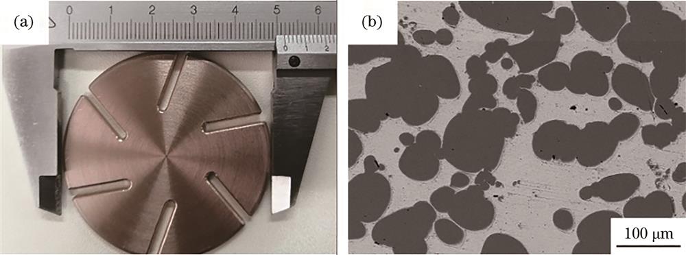
    Fig. 1. CuCr50 alloy. (a) Contact specimen; (b) microstructure
    Schematic diagram of laser surface remelting experimental system
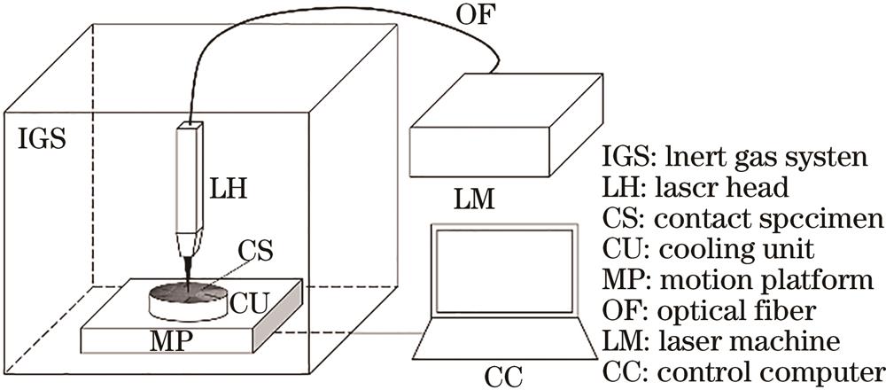
    Fig. 2. Schematic diagram of laser surface remelting experimental system
    Cross-sectional microstructure of the remelting layer of CuCr50 alloy. (a) Overall view; (b) local magnified image
    Fig. 3. Cross-sectional microstructure of the remelting layer of CuCr50 alloy. (a) Overall view; (b) local magnified image
    SEM images of remelting layer under different scanning speeds. (a) 2000 mm/min; (b) 4000 mm/min; (c) 6000 mm/min; (d) 8000 mm/min; (e) 10000 mm/min
    Fig. 4. SEM images of remelting layer under different scanning speeds. (a) 2000 mm/min; (b) 4000 mm/min; (c) 6000 mm/min; (d) 8000 mm/min; (e) 10000 mm/min
    Influence of scanning speed on the depth of remelting layer
    Fig. 5. Influence of scanning speed on the depth of remelting layer
    Influence of scanning speed on microhardness distribution of remelting layer
    Fig. 6. Influence of scanning speed on microhardness distribution of remelting layer
    Fracture morphology and element distribution map. (a) Remelting layer; (b) substrate
    Fig. 7. Fracture morphology and element distribution map. (a) Remelting layer; (b) substrate
    Laser processing parametersValue

    Scanning speed /

    (mm·min-1

    2000,4000,6000,8000,10000
    Laser power /W530
    Spot diameter /mm0.09
    Overlapping rate /%20
    Table 1. Processing parameters of laser surface modification process
    Scanning speed /(mm·min-1200040006000800010000Original
    Ra /μm>105.495.275.063.340.81
    Table 2. Relationship between scanning speed and surface roughness of CuCr50
    Scanning speed /(mm·min-1400060008000Original
    Yield strength /MPa233225212182
    Table 3. Tensile property parameters of laser treated and original specimens
    Xu Wang, Gang Yu, Xiuli He, Shaoxia Li, Chongxin Tian, Jiayun Shao, Baohua Liu. Effect of Scanning Speed on Properties of Laser Surface Remelting Layer of CuCr Alloy[J]. Laser & Optoelectronics Progress, 2022, 59(1): 0114006
    Download Citation