
Yaoyao Lu, Daolin Cai, Yifeng Chen, Shuai Yan, Lei Wu, Yuanguang Liu, Yang Li, Zhitang Song. Improving the data retention of phase change memory by using a doping element in selected Ge2Sb2Te5[J]. Journal of Semiconductors, 2019, 40(4): 042402
- Journal of Semiconductors
- Vol. 40, Issue 4, 042402 (2019)
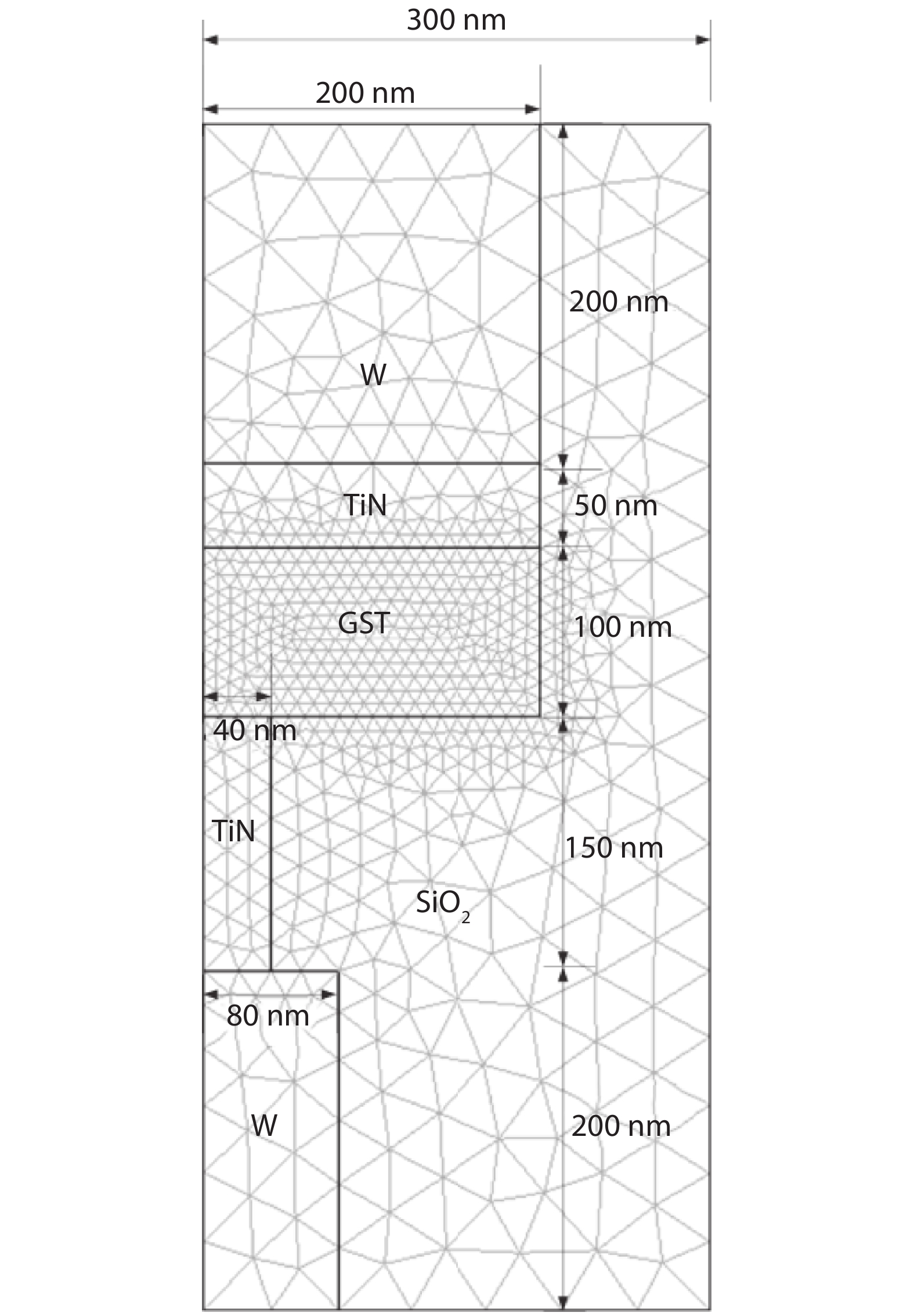
Fig. 1. (Color online) Geometries and schematic cross section of the T-shaped PCM cell.
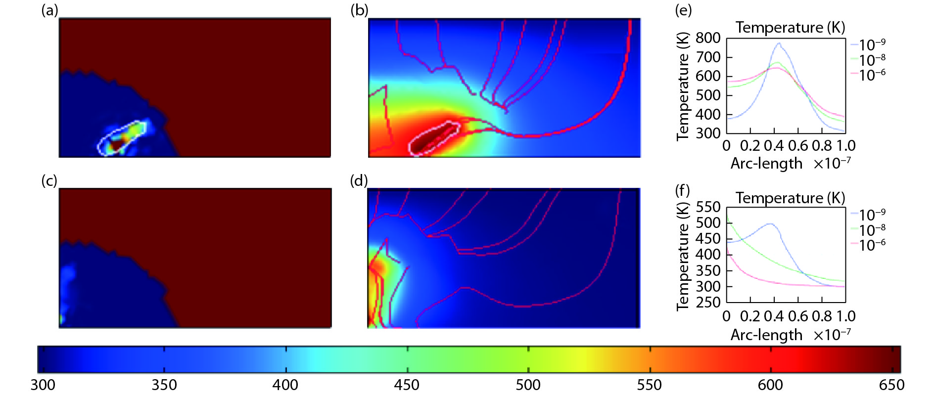
Fig. 2. (Color online) The crystalline domain (light color) among amorphous phase (dark blue) under current pulses of (a) 0.5 mA/1 μ s and (b) 0.01 mA/1 μ s; the temperature distributions and current density distributions under current pulses of (c) 0.5 mA/1 μ s and (d) 0.01 mA/1 μ s; the temperature values along horizontal direction (r -axis) under current pulses of (e) 0.5 mA/1 μ s and (f) 0.01 mA/1 μ s, the time points vary from 1 ns (blue line) to 1 μ s (red line), the median time point is 10 ns (green line).
Fig. 3. (Color online) Temperature profiles of selective points along horizontal direction (r -axis) during current pulse: lines are presented under current amplitude of 0.5 mA whereas solid symbols are presented under current amplitude of 0.01 mA; points at coordinate (z = 360 nm, r = 0 nm) are expressed in black, points at coordinate (z = 360 nm, r = 20 nm) are expressed in blue, and points at coordinate (z = 360 nm, r = 40 nm) are expressed in pink. To facilitate the observation and comparison, the figure zooms in 60 ns. The entire temperature profiles are showed in insert figure.
Fig. 4. (Color online) Geometries and schematic cross sections of the PCM cell with incremental doped radius.
Fig. 5. (Color online) The temperature distributions of RESET operation for the PCM cells with incremental doped radius.
Fig. 6. (Color online) Variations of resistance as a function of programming current amplitudes in RESET operations for the PCM cell with incremental doped radius.
Fig. 7. (Color online) The temperature distributions and current density distributions of SET operation for the PCM cell with incremental doped radius.
Fig. 8. (Color online) The temperature distributions and current density distributions at electrical pulse of 0.01 mA and 1 μ s of the PCM cells with different radius of doped regions: (a) r = 10 nm, (c) r = 20 nm, (e) r = 30 nm and (g) r = 40 nm. The results after increasing current pulse width to 10 μ s, (b), (d), (f) and (h) correspond to (a), (c), (e) and (g) respectively.
Fig. 9. (Color online) Temperature profiles of the selective point (z = 380 nm, r = 0 nm) during current pulse: lines are presented under current duration of 1 μ s whereas solid symbols are presented under current duration of 10 μ s; the temperature changes of doped radius r = 10 nm are expressed in black, the temperature changes of doped radius r = 10 nm are expressed in blue, and the temperature changes of doped radius r = 10 nm are expressed in pink. To facilitate the observation and comparison, the figure zooms in the graphics within 80 ns.
|
Table 1. Physical properties of materials used in numerical simulation.
|
Table 2. The correlation coefficients of JMAK equation used in numerical simulation.
|
Table 3. Physical properties of N doped GST used in numerical simulation.

Set citation alerts for the article
Please enter your email address
© Copyright 2018-2021 | Chinese Laser Press. All Rights Reserved 沪ICP备15018463号-20