
Yaoyao Lu, Daolin Cai, Yifeng Chen, Shuai Yan, Lei Wu, Yuanguang Liu, Yang Li, Zhitang Song. Improving the data retention of phase change memory by using a doping element in selected Ge2Sb2Te5[J]. Journal of Semiconductors, 2019, 40(4): 042402
- Journal of Semiconductors
- Vol. 40, Issue 4, 042402 (2019)
Abstract
1. Introduction
Phase change memory (PCM) has emerged as a promising candidate for future non-volatile memory (NVM) thanks its low power consumption, fast operating speed, high storage density and multi-bit per cell (MLC) storage capability[
The material-transport-related switching of PCM is nonvolatile, even when not powered; however, it also has several reliability issues[
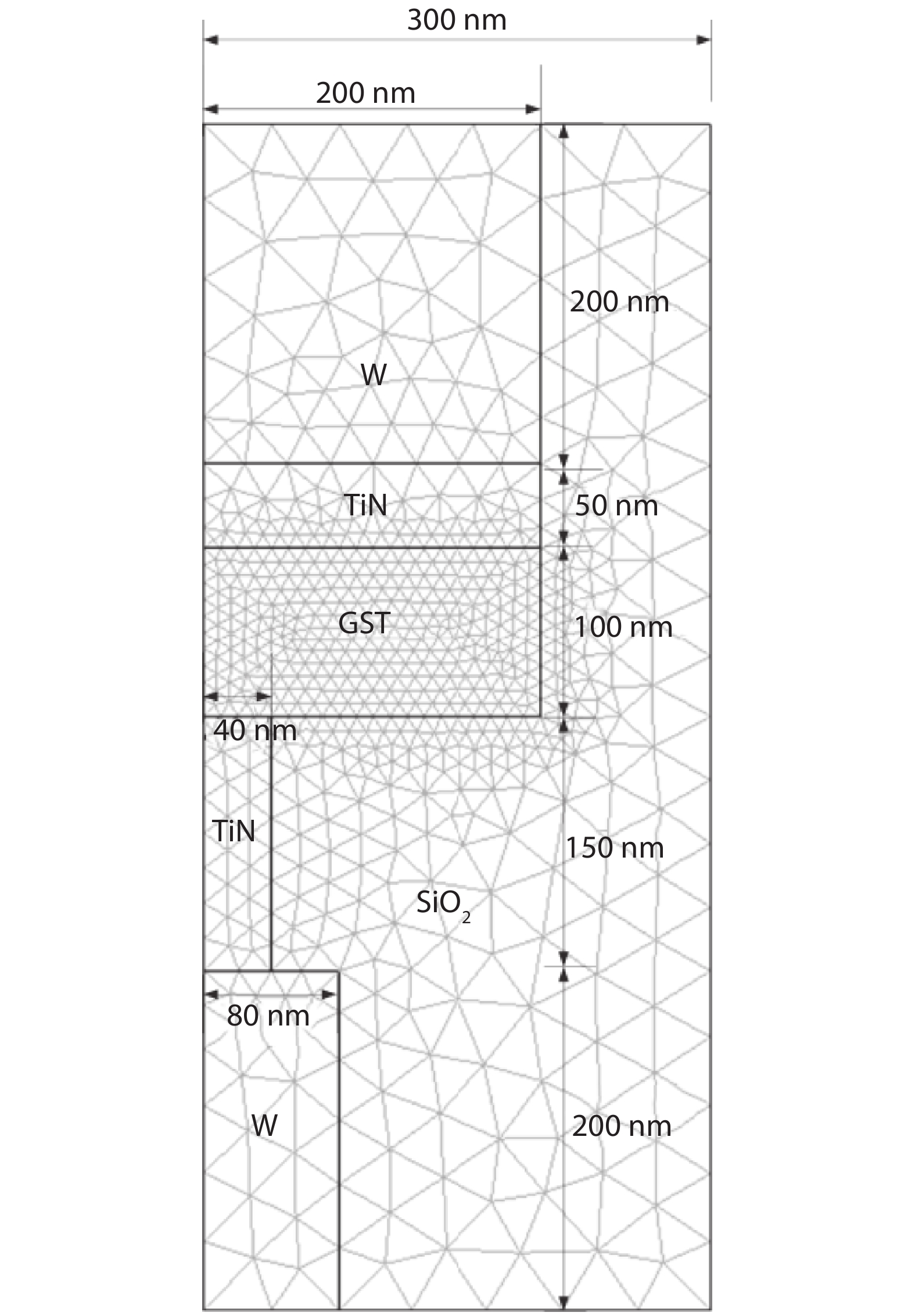
2. Finite element model
A numerical simulation model of a T-shaped PCM cell has been established with rotational symmetry, as shown in Fig. 1, consisting of sandwich structure as W/TiN/GST/TiN/W. SiO2 was chosen as the isolation material surrounding the electronic contact and phase change layer. In this paper, the material and size parameters of each layer were in good conformity with the real PCM cell[
![]()
Figure 1.(Color online) Geometries and schematic cross section of the T-shaped PCM cell.
The Joule heating and electric current modules were coupled such that the current continuity (1) and heat transport (2) equations could be solved self-consistently[
where J is the electrical current density, σ is the electric conductivity, V is the electric potential, ρ is the density, T is the temperature, C is the heat capacity, k is the thermal conductivity, t is the time and Q is the heat flux, which could be expressed as
Table 1[
For the RESET operation, the initial crystalline PCM cell is heated above melting temperature (893 K) and is then quenched rapidly (faster than the crystallization speed) to switch the molten meshes into amorphous phase. Based on the calculations of previous step, the SET current pulse and small disturb current pulse are applied to the PCM cell to simulate the crystallization process. Unfortunately, the mechanism of crystallization is still controversial. Among the existing descriptions of crystallization kinetics[
where t is time, n is the Avrami coefficient, and K is an effective rate constant. Theoretically, the Avrami coefficient should be an integer providing information on the dimensionality of the crystallization process. The effective rate constant describing the nucleation and growth rates is generally given by an Arrhenius equation
where v is the frequency factor, EA is the activation energy,T is the absolute temperature, and kB is the Boltzmann constant. The correlation coefficients of the JMAK equation are listed in Table 2[
3. Simulation results and discussion
The RESET current pulse of 2.6 mA and 300 ns is applied to the initial crystallization PCM cell and heating a hemispherical phase change region switches it into the amorphous phase. The minimum SET current pulse can be calculated based on the JMAK equation which would crystallize the amorphous domain once it has reached the crystallization temperature (653 K). By combining Eqs. (2), (6) and (7), the minimum SET current is calculated as 0.335 mA. To manifest the crystallization process better, the SET current amplitude is set to 0.5 mA. Since the amorphous region presents as hemispherical, the resistivity of solving domain is growing towards the symmetry axis. This means that Joule heat would diffuse from the edge of the bottom electric contact (BEC), where the current density convergences at the very start due to edge effect, to the direction of symmetry axis. Furthermore, when the edge effect of current density could be negligible under the small disturb current pulse, the symmetry axis of the amorphous region is most likely to crystallize, because the larger resistivity would generate more Joule heat under the almost same current density. This process requires a sufficiently small current. Therefore, in this work, 0.01 mA is chosen as the amplitude of disturb current pulse.
After the RESET operation on the PCM cell, the SET pulse of 0.5 mA and 1 μs and the small disturb current pulse of 0.01 mA and 1 μs are applied respectively. The corresponding crystallization conditions are displayed in Fig. 2. The crystallization path (marked by white circle) shunting down the amorphous region (dark blue) appears around the corner of BEC under SET pulse, as shown in Fig. 2(a), which successfully switches the PCM cell from 1.268 MΩ to 755 Ω. Fig. 2(c) illustrates the temperature and current density distributions under SET current pulse. By consulting the color map at the bottom of figure it can be seen that the region with the highest temperature occurs at the region where the most intensive current density (red lines) assembles. Thus, the crystallization process under SET current could be re-performed as: the current density converged at the edge of the BEC is strong enough to crystallize the amorphous domain, and these crystallized meshes own the conductivity four orders of magnitude larger than the surrounding amorphous GST. Consequently, they would attract more current to continue the crystallization process. In the end, the crystallization path is located at the corner of BEC. Fig. 2(e) verifies this interpretation. The minute the SET current is applied, the temperature at the edge of BEC (r-axis coordinate is 40 nm) rises to 741 K (see blue line in Fig. 2(e)). The temperature of this point always maintains the highest during SET current duration, accompanied by heat diffusion to symmetry axis, as shown in green and red lines. The existing heat diffusion among amorphous domain may account for the heat accumulation at the symmetry axis, resulting in crystallization under small disturb current pulse, see Fig. 2(b), which is detrimental to the data retention of high-resistance state. The temperature distributions in Fig. 2(d) clearly dictate the heat aggregation at the symmetry axis under the small disturb current pulse. Temperature evolution recurs in Fig. 2(f). Like the SET operation, the temperature surges firstly at the edge of BEC. However, this energy is insufficient to drive crystallization. Subsequently, the heat diffuses outwards and the temperature at symmetry axis increases. Note that the crystallization ratio is a function of temperature and time. Thus the crystallization behavior would happen under a small disturb current though the temperature in entire phase change layer could not achieve the crystallization temperature.
![]()
Figure 2.(Color online) The crystalline domain (light color) among amorphous phase (dark blue) under current pulses of (a) 0.5 mA/1
To further understand the temperature changes during the current pulses, Fig. 3 provides the temperature profiles of selective points (360, 0), (360, 20) and (360, 40) (unit: nm) under these two types of current pulses. The temperatures under 0.5 mA SET current pulse end in higher levels than the temperatures under 0.01 mA disturb current pulse. The temperature increases along horizontal direction under SET current pulse, for the current flows through crystallization path located at the corner of BEC. While the temperature changes under small disturb current pulse show opposite trend. The temperatures of these three points experience peaks following the application of 0.01 mA small current. After about 10 ns, the temperatures tend to be stable, exhibiting the trend of decay along horizontal direction.
![]()
Figure 3.(Color online) Temperature profiles of selective points along horizontal direction (
4. Incremental N-doped radius
The distinguished tendency of temperature changes under these two current pulses could lead to different crystallization regions. Based on the disparate crystallization path, a new structure for phase change layer is proposed. As shown in Fig. 4, the nitrogen (N) element is doped in the symmetry axis of GST, ascending the crystallization temperature of doped area to 720 K. The other key parameters of N-doped GST[
![]()
Figure 4.(Color online) Geometries and schematic cross sections of the PCM cell with incremental doped radius.
Table Infomation Is Not EnableFig. 5 offers the temperature contours with incremental doped radius after RESET operation by RESET current pulse of 1.7 mA and 300 ns. The PCM cell with traditional structure could not achieve enough amorphous volume to cover up the BEC, whereas the PCM cells with new structure are capable of forming a mushroom amorphous region in the phase change layer to reach high-resistance state. Furthermore, the hotspots have a higher temperature and the amorphous volumes increase with incremental doped radius. The amorphous N-doped GST possesses larger resistivity thus generates more Joule heat to melt phase change materials, which could account for such superior property for new structure. However, the hotspots located in BEC would lower the heat efficiency of RESET operation. The programming curve (R–I) depicted in Fig. 6 illustrates that PCM cells with incremental doped radius exhibit more excellent performance, such as smaller RESET current, larger margin between two resistance states, and so on.
![]()
Figure 5.(Color online) The temperature distributions of RESET operation for the PCM cells with incremental doped radius.
![]()
Figure 6.(Color online) Variations of resistance as a function of programming current amplitudes in RESET operations for the PCM cell with incremental doped radius.
Meanwhile, the SET operation is unaffected by the PCM cells with incremental doped radius, as shown in Fig. 7, because the SET current of 0.5 mA and 1 μs could perfectly switch the cells to about 700 Ω. Note that this resistance is much smaller than the experimental value, because the simulation model in this paper optimizes the cell’s structure defects.
![]()
Figure 7.(Color online) The temperature distributions and current density distributions of SET operation for the PCM cell with incremental doped radius.
The temperature and current density distributions under small disturb current pulse of 0.01 mA and 1 μs are presented in Figs. 8(a), 8(c), 8(e) and 8(g), to verify that new structure could play a role in improving data retention. As the results show, the positions of hotspots no longer appear at symmetry axis but are located outwards of the doped region with a maximum temperature (630 K) that is lower than the crystallization temperature. The resistances obtained are 150, 867, 844 and 777 kΩ for doped radius r = 10, r = 20, r = 30 and r = 40 (unit: nm) respectively. Compared with the result 82.9 kΩ from traditional PCM cell under current of 0.01 mA and 1 μs, all the resistances from new structures are above 100 kΩ—the boundary discriminates high-resistance state and low-resistance state. Extending the disturb current duration to 10μs, the temperature and current density distributions are shown in Figs. 8(b), 8(d), 8(f) and 8(h). The resistances after current application are 132, 271, 197 and 901 kΩ corresponding doped radius r = 10, r = 20, r = 30 and r = 40 (unit: nm) respectively. Comparing the two images up and down, the positions of hotspots are barely changed, while the maximum temperature descends to 360 K. The resistances significantly decrease because the cumulative time augments crystallization ratio. An exception appears when doped radius reaches 40 nm that the resistance does not reduce but ascend, which might involve the degradation process of nuclei according to classic nucleation theory. Further analysis for the heat changes versus time are presented in Fig. 9. The point (z = 380 nm, r = 0 nm) is selected to represent the temperature profile at symmetry axis. With doped volume increases, the heat decreases. The resistivity of amorphous N-doped GST is one order of magnitude larger than the pure amorphous GST, which would cause the current density distances itself from the symmetry axis. And this trendy basically remains valid with enlarged current duration, except that temperature generated in PCM cell with doped radius r = 40 nm grows gradually, which could be interpreted as a low current produces a tremendous heat in so large an amorphous domain.
![]()
Figure 8.(Color online) The temperature distributions and current density distributions at electrical pulse of 0.01 mA and 1
![]()
Figure 9.(Color online) Temperature profiles of the selective point (
Based on these simulation results, the PCM cell with doped radius r = 40 nm exerts a better performance. It could effectively reduce RESET current to 1.3 mA, and widen resistance window nearly three times more than traditional PCM cell. It also presents outstanding performance in terms of resisting small current interference existed in circuit because the resistance under 0.01 mA current pulse only decreases to 777 kΩ, which is far more than failure resistance 100 kΩ. The increased resistance under prolonged current duration illustrates that it could be used to promote the PCM cell’s data retention. Note that the doped radius exceeding the size of BEC is not mentioned in this work because they potentially influence SET process in real work.
5. Conclusion
The crystallization characteristics of a T-shaped PCM cell based on typical chalcogenide GST, under SET current pulse (0.5 mA) and very small disturb current pulse (0.01 mA), have been investigated by finite element modelling. According to the distributions of temperature and current density, the crystallization region under SET current pulse presents first at the edge of the BEC. It then promptly forms a filament shunting down the amorphous phase to achieve the low-resistance state, whereas the tiny disturb current pulse accelerates crystallization at the symmetry axis in the phase change material. Considering these different crystallization paths, a new structure of phase change material layer, configured by doping N element into pure GST in confined region, is proposed to hinder the crystallization behavior under small disturb current pulse while ensuring a normal crystallization process under SET current pulse. This new structure is designed to improve the data retention for PCM cell by increasing the crystallization temperature to 720 K for the symmetry axis area, where it is filled with N-doped GST. The electrical-thermal characteristics of incremental doped radius, from 10 to 40 nm, have been analyzed. It can be concluded that the PCM cell with doped radius r = 40 nm thas a better performance, such as smaller RESET current 1.3 mA, wider window between high resistance of 3.2 MΩ and low resistance of 750 Ω, and better anti-disturb ability concerning small current pulse.
Acknowledgements
The authors would like to acknowledge the support of the "Strategic Priority Research Program" of the Chinese Academy of Sciences (No. XDA09020402), the National Integrate Circuit Research Program of China (No. 2009ZX02023-003), the National Natural Science Foundation of China (Nos. 61261160500, 61376006, 61401444, 61504157), the Science and Technology Council of Shanghai (Nos. 14DZ2294900, 15DZ2270900, 14ZR1447500), and the National Natural Science Foundation of China (61874178).
References
[1] S Lai. Current status of the phase change memory and its future. IEEE International Electron Devices Meeting, 255(2003).
[2] S R Ovshinsky. Reversible electrical switching phenomena in disordered structures. Phys Rev Lett, 21, 1450(1968).
[3] Z M Sun, J Zhou, R Ahuja. Structure of phase change materials for data storage. Phys Rev Lett, 96, 055507(2006).
[4] S Raoux, W Welnic, D Ielmini. Phase change materials and their application to nonvolatile memories. Chem Rev, 110, 240(2009).
[5] K Kohary, C D Wright. Electric field induced crystallization in phase-change materials for memory applications. Appl Phys Lett, 98, 223102(2011).
[6] J M Li, H M Yang, K G Lim. Field-dependent activation energy of nucleation and switching in phase change memory. Appl Phys Lett, 100, 263501(2012).
[7]
[8] D L Cai, H P Chen, Q Wang et al. An 8-mb phase-change random access memory chip based on a resistor-on-via-stacked-plug storage cell. IEEE Electron Device Lett, 33, 1270(2012).
[9] Y Liu, Z T Song, Y Ling et al. Three-dimensional numerical simulation of phase-change memory cell with probe like bottom electrode structure. Jpn J Appl Phys, 48, 024502(2009).
[10] Z Xu, B Liu, Y F Chen et al. The improvement of nitrogen doped Ge2Sb2Te5 on the phase change memory resistance distributions. Solid-State Electron, 116, 119(2016).
[11] W A Johnson, R F Mehl. Reaction kinetics in processes of nucleation and growth. Trans Metall Soc AIME, 135, 416(1939).
[12] M Volmer, A Weber. Keimbildung in übersättigten Gebilden. Zeitschrift für physikalische Chemie, 119, 227(1926).
[13] S Senkader, C D Wright. Models for phase-change of Ge2Sb2Te5 in optical and electrical memory devices. J Appl Phys Lett, 95, 504(2004).
[14] J H Bae, B G Kim, D S Byeon et al. Simulation for thickness change of PRAM recording layer. J Ceram Soc Jpn, 117, 588(2009).
[15] Y F Gong, Z T Song, Y Ling et al. Simulation of voltage SET operation in phase-change random access memories with heater addition and ring-type contactor for low-power consumption by finite element modeling. Chin Phys Lett, 27, 068501(2010).

Set citation alerts for the article
Please enter your email address
© Copyright 2018-2021 | Chinese Laser Press. All Rights Reserved 沪ICP备15018463号-20