• Laser & Optoelectronics Progress
  • Vol. 57, Issue 3, 032202 (2020)
Yi Yin1, Zhijian Liu1、*, Saijie Wang1, Sen Wu1, Zhijun Yan1, and Xinxiang Pan2
Author Affiliations
  • 1Marine Engineering College of Dalian Maritime University, Dalian, Liaoning 116026, China
  • 2College of Ocean Engineering, Guangdong Ocean University, Zhanjiang, Guangdong 524088, China
  • show less
    DOI: 10.3788/LOP57.032202 Cite this Article Set citation alerts
    Yi Yin, Zhijian Liu, Saijie Wang, Sen Wu, Zhijun Yan, Xinxiang Pan. High-Precision ITO Electrode Wet Etching Technology Based on Maskless Lithography[J]. Laser & Optoelectronics Progress, 2020, 57(3): 032202 Copy Citation Text show less
    Diagram of production process. (a) Pouring; (b) spin coating; (c) exposure; (d) development; (e) etching; (f) removing glue
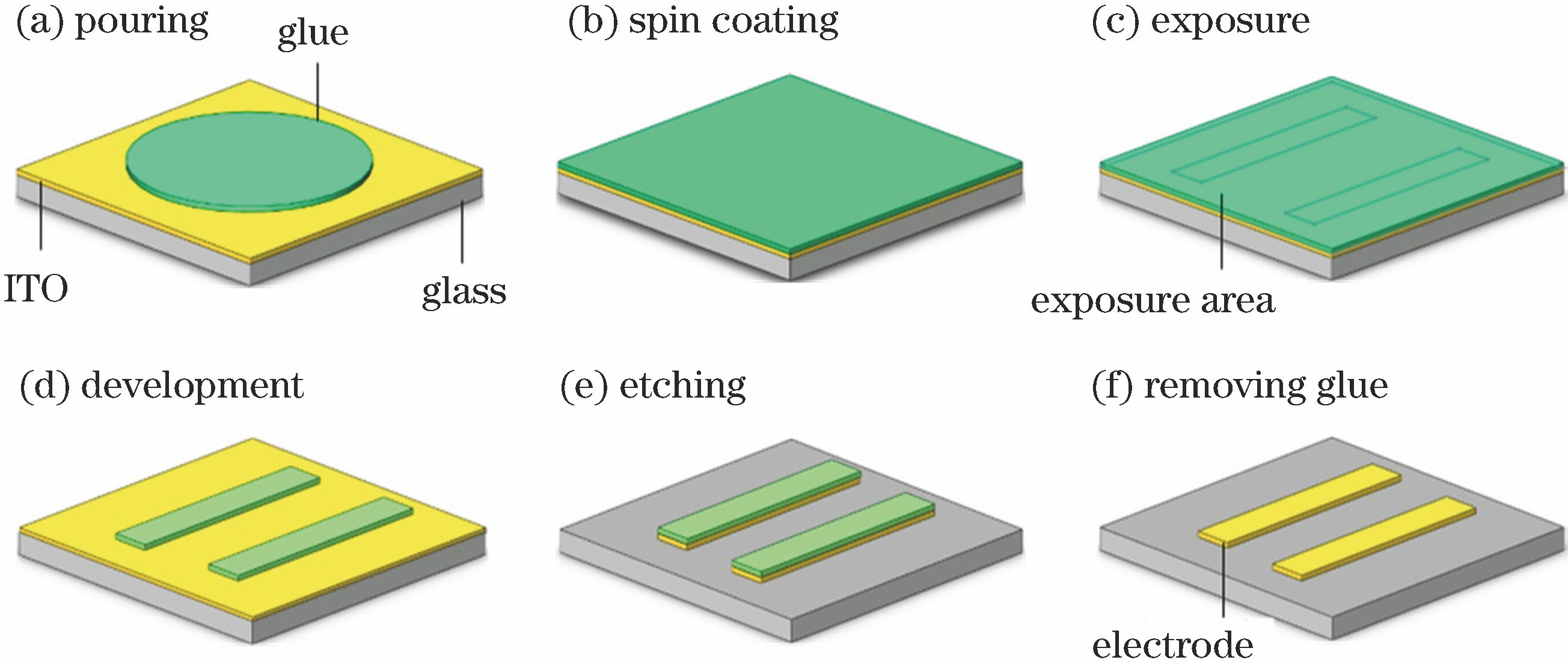
    Fig. 1. Diagram of production process. (a) Pouring; (b) spin coating; (c) exposure; (d) development; (e) etching; (f) removing glue
    Morphologies of photoresist after different development time. (a) 25 s; (b) 30 s; (c) 35 s
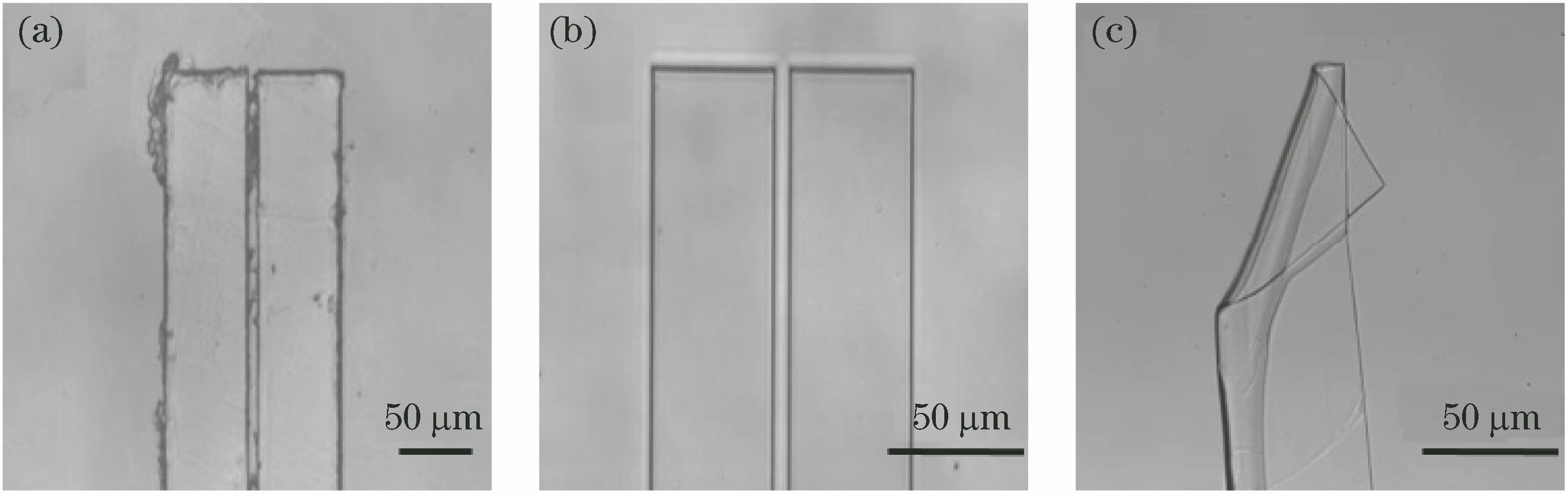
    Fig. 2. Morphologies of photoresist after different development time. (a) 25 s; (b) 30 s; (c) 35 s
    Electrode morphologies after different etching time. (a) 180 s; (b) 210 s; (c) 240 s
    Fig. 3. Electrode morphologies after different etching time. (a) 180 s; (b) 210 s; (c) 240 s
    Comparison of photoresist morphologies with different sizes after development. (a) 200 μm; (b) 100 μm; (c) 50 μm; (d) 20 μm; (e) 10 μm; (f) 2 μm
    Fig. 4. Comparison of photoresist morphologies with different sizes after development. (a) 200 μm; (b) 100 μm; (c) 50 μm; (d) 20 μm; (e) 10 μm; (f) 2 μm
    Comparison of electrode effects with different size after glue removal. (a) 200 μm; (b) 100 μm; (c) 50 μm; (d) 20 μm; (e) 10 μm; (f) 2 μm
    Fig. 5. Comparison of electrode effects with different size after glue removal. (a) 200 μm; (b) 100 μm; (c) 50 μm; (d) 20 μm; (e) 10 μm; (f) 2 μm
    2 μm electrode morphology under atomic force microscope
    Fig. 6. 2 μm electrode morphology under atomic force microscope
    Cross-sectional shape curves of 2 μm electrode and glass substrate under atomic force microscope
    Fig. 7. Cross-sectional shape curves of 2 μm electrode and glass substrate under atomic force microscope
    Yi Yin, Zhijian Liu, Saijie Wang, Sen Wu, Zhijun Yan, Xinxiang Pan. High-Precision ITO Electrode Wet Etching Technology Based on Maskless Lithography[J]. Laser & Optoelectronics Progress, 2020, 57(3): 032202
    Download Citation