Abstract
We report the fabrication details of a monolithically integrated electro-absorption modulated distributed feedback laser (EML) based on the ion-implantation induced quantum well intermixing (QWI) technique. To well-preserve material quality in the laser region, thermal-oxide is deposited before implantation and the ion-implantation buffer layer is etched before annealing. Thirteen pairs quantum well and barrier are employed to compensate deterioration of the modulator’s extinction ratio (ER) caused by the QWI process. The fabricated EML exhibits an 18 dB static ER at 5 V reverse bias. The 3 dB small signal modulation bandwidth of modulator is over 13.5 GHz indicating that this EML is a suitable light source for over 16 Gb/s optical transmission links.Monolithically integrated electro-absorption modulated distributed feedback lasers (EMLs)[1–3] consisting of an electro-absorption (EA) modulator and a distributed feedback (DFB) laser is widely used as the most essential and promising light source in optical transmission links and systems. Besides possessing advantages of an EA modulator[4], such as high speed, low chirp, smaller size, and low driving voltage, the integrated EML has high coupling efficiency between the modulator and laser leading to a high output power of the modulated light.
Material integration is the first and key step for fabrication of an EML. A conventional method is the butt-joint technique[5,6] which needs to regrow material by the epitaxy process to achieve integration of different band edges materials. Although this method does possess high flexibility, it is challenging to obtain low reflection and optical loss at the material interface. Another approach is the selective-area growth (SAG) technique[7,8], in which is easily to realize multiple band edges across a wafer without multiple epitaxial growths and a core-layer material etching processes. However, the abruptness of the transition region and varied thickness of the epitaxial material by the SAG technique are not ideal. The quantum well intermixing (QWI) technique[9], which does not need to regrow material, is a relatively simple method and employed in this work. Because the QWI process only slightly changes the compositional profile rather than the average composition, there is a negligible index discontinuity at the interface between adjacent regions. By using this integration scheme, the laser and modulator can be simultaneously optimized for high performance with relatively simple fabrication procedures.
In our work, we used a simple and robust phosphorus ion () implantation-induced QWI process to fabricate an EML. By depositing an implantation mask and etching ion-implantation buffer layer, the material of the laser region has been well-preserved with only a 4.3 nm blue shift. An undoped-InP annealing protection layer was also inserted to protect the upper separate confinement heterostructure (SCH) of the laser during the rapid-thermal-anneal (RTA) process. The depth of intermixing is controlled by using the temperature, annealing time, implant energies, and implant dose[9,10]. The fabricated EML exhibits an 18 dB static extinction ratio (ER) at 5 V reverse bias. The 3 dB small signal modulation bandwidth of the EA modulator is over 13.5 GHz. The effect of the QWI process on the Fabry–Pérot (FP) laser threshold current density, fabrication details of EML, and further approaches to improve the ER are presented and discussed, respectively.
Sign up for Chinese Optics Letters TOC. Get the latest issue of Chinese Optics Letters delivered right to you!Sign up now
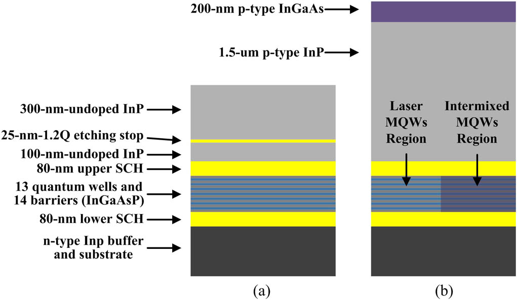
Figure 1(a) shows the epitaxial structure for QWI process. It can be seen that the multiple quantum wells (MQWs) consists of 13 compressively strained InGaAsP wells (, , where the subscript PL stands for photoluminescence) and 14 tensile strained InGaAsP barriers (, ). The entire MQWs has compressive strain with . In the intermixed wells, the initial square quantum well (QW) potential profile is reshaped into a parabolic shape with low carrier confinement in the MQWs layer, which leads to deterioration of the exciton absorption[11]. A large optical confinement factor in the MQWs layer would compensate for that deterioration by increasing the number of QW as in our device. On the MQWs, 80 nm 1.2Q InGaAsP upper SCH, 100 nm undoped InP, 25 nm 1.2Q InGaAsP, and 300 nm undoped InP are grown by metal-organic vapor-phase epitaxy (MOVPE), successively. The 300 nm undoped InP was used as implantation buffer layer in order to trap ions in the modulator region. The 25 nm 1.2Q InGaAsP and 100 nm undoped InP are the etching stop layer and annealing protection layer for the laser regions, respectively. The main purpose of using an annealing protection layer is to protect the upper SCH layer of the laser. Without this layer, the upper SCH layer would be directly covered by and some defects from the and etching processes would easily diffuse into the SCH layer during the RTA process.

Figure 1.(a) Epitaxial structure for QWI process; (b) final regrowth structure.
The QWI process was used to decrease the bandgap wavelength in the modulator region. The QWI process was achieved by implantation, which generates point defects in the implantation buffer layer, and the RTA process. During the RTA process, the introduced point defects diffuse into and throughout the MQWs. At the heterojunction interface, the point defects help in enhancing composition interdiffusion. As a result, the potential profile of the QW would be changed from a square shape to a parabolic shape causing a blue shift of the bandgap wavelength. Figure 2 shows a schematic diagram of implantation QWI with an etching implantation buffer layer. First, implantation was selectively performed with 400 nm thermal-oxide implantation mask to introduce point defects into the undoped InP implantation buffer layer. Then, the implantation buffer layer of the laser region was removed and 200 nm plasma-enhanced chemical vapor deposition was deposited on the surface of the entire wafer for prevention phosphorus atoms separating out during the RTA process. After RTA process with appropriate conditions, the desired band edge of the EA modulator region was defined. Distinct from the traditional implantation QWI process[12], a 100 nm undoped InP annealing protection layer was introduced and an extra etching implantation buffer layer process was implemented within the QWI process employed in this work. By well-controlling the implantation energy and dose, all implanted ions would be trapped into the buffer layer of the EA region. In the laser region, most of implanted ions were stopped in thermal-oxide and the residual were cleaned up by the etching buffer layer process.
Figure 2.Schematic diagram of implantation QWI with etching implantation buffer layer. From left to right, implantation, etch implantation buffer layer, and RTA process.
Figure 3 shows the PL peak shift as a function of anneal time for a RTA temperature of 645°C of different samples. Samples 1 and 2 have same epitaxial structure as shown in Fig. 1(a). During the implantation process, Samples 1 and 2 are masked and unmasked by the 400 nm thermal-oxide , respectively. Sample 3 is processed by the traditional implantation QWI process. The difference between Samples 3 and 2 is that Sample 3 has no 100 nm undoped-InP annealing protection layer and extra etching implantation buffer layer process. implantation was performed at an energy of 50 keV, with a dose of , and at substrate temperature of 200°C. As can be seen, the PL peak shift of the -masked sample with an etching ion-implantation buffer layer is 11 nm which is much lower than that of the traditional implantation QWI technique under the 360 s RTA process. This blue shift is caused by pure thermal diffusion at the heterojunction interface. In this work, we choose 70 s and 645°C as the RTA condition to obtain the desired blue shift of the modulator region. As illustrated in Fig. 4, a 65.1 nm PL peak wavelength detuning between the laser and modulator regions would be obtained and the blue shift in the laser region is only 4.3 nm indicating that high material quality has been well-preserved.
Figure 3.PL peak shift as a function of anneal time of different samples.
Figure 4.PL spectrum of laser and modulator regions.
After the QWI process, the implantation buffer layer, etching stop layer, and 100 nm undoped InP were removed. The gratings with a uniform pitch were fabricated by holographic lithograph for th DFB laser. Then, a second MPOVE growth step was performed, in which the cladding layer and contact layer were grown [Fig. 1(b)]. Next, the wafer was subjected to definition and etching waveguides, and a 3 μm surface-ridge waveguide with a reverse-mesa-ridge structure was fabricated by wet chemical etching to ensure a low capacitance of the modulator and a small series resistance of the laser. To guarantee the accurate height of the ridge, there were two wet-chemical-etching steps: in the first step, we used solution to etch 200 nm InGaAs; then, HCl and mixture solution was used to etch 1.5 μm InP and the etching stops at upper SCH layer because the solution does not etch InGaAsP. To suppress electronic crosstalk between the laser and modulator, a p-type InGaAs contact layer was removed from the isolation region and helium ion () implantation was performed. A 400 nm thermal-oxide was deposited on the entire wafer as an insulator and an window over the ridges was formed by using HF solution. A polyimide pad was formed for the modulator electrode pad to reduce parasitical capacitance. Next, Ti/Au was sputtered on the top of the wafer to fabricate p-contact electrodes for the different sections of the device. At the end of the fabrication, Au/Ge/Ni alloy was evaporated as a common n-contact electrode of the device after the wafer was thinned to 150 μm. After the fabrication processes were completed, the wafer was cleaved into individual dies and each die was coated with an antireflection (AR) coating and a high-reflection (HR) coating. Then the device was test after sintering on a Cu heat sink controlled by a thermoelectric cooler (TEC).
Figure 5 shows the optical microscope image of the fabricated device with section indications. To balance the ER and high-frequency response, the EA modulator is 140 μm long and the DFB laser is 300 μm long. Between the laser and modulator regions, there is a 50 μm long electrical isolation region. All tests in this work are under 25°C controlled by TEC. The FP cavity reflection spectrum method[13] has been used to measure the EA modulator waveguide loss at a wavelength of 1528 nm. The waveguide loss is about , which corresponds to an insertion loss under 0.8 dB for the 140 μm long EA modulator without bias at 1528 nm. Figure 6 shows the light output power versus injection current () characteristic curves of the EML without bias in the EA modulator, 270 μm long as-grown FP laser, and 270 μm long implanted FP laser with same PL peak blue shift as the EA modulator. It can be seen that the implanted FP laser’s threshold current density has increased to when compared with the as-grown one, whereas the slope efficiencies of both lasers remain comparable. This increase can be explained in part by the loss of carrier confinement in the intermixed wells. The composition interdiffusion at the heterojunction interfaces is enhanced when point defects diffusing throughout the MQWs, which results in a controlled reshaping of the initial square QW potential profile into a wider, shallower, and more parabolic shape that has low carrier confinement[11]. In addition, implantation damage not fully treated during the RTA process[14] and optical scattering from implanted ions might be other factors. The optical spectrum of the EML is shown in Fig. 6, inset. The lasing wavelength is 1527.6 nm with a 47 dB side-mode suppression ratio under an 80 mA injection current. Furthermore, we have measured the linewidth of the EML by the delayed self-heterodyne method. The Lorentz fitting linewidth value is 3.7 MHz.
Figure 5.Optical microscope image of the fabricated device with section indications.
Figure 6. curves of as-grown FP laser, implanted FP laser, and EML without bias. Inset, optical spectrum of the device.
Static ER as an important characteristic of EML also was tested (Fig. 7). With a 5 V reverse voltage in an EA modulator and an 80 mA injection current in a DFB laser, the device exhibits 18 dB ER with a peak extinction efficiency of at . To further improve the static ER of the intermixed-MQWs EA modulator, the MQWs structure must be fine designed, such as well depth and width, barrier band gap, and strain[15]. Additionally, wavelength detuning between the EA modulator exciton peak and laser lasing wavelength is also crucial for a tradeoff between the ER and output power of intermixed-MQWs EML. It should be noted that the peak extinction efficiency of the intermixed MQWs is lower than that of as-grown MQWs within a narrow wavelength range[11]. Thus, a relatively high reverse voltage is inevitable in order to obtain a certain ER value.
Figure 7.Static ER and extinction efficiency as functions of bias voltage.
A 50 GHz network analyzer is used for measurement of the small signal frequency response of the fabricated EA modulator. The normalized electrical-to-optical response of the modulator is shown in Fig. 8. It can be seen that the 3 dB small signal modulated bandwidth is over 13.5 GHz, which is enough for up to 16 Gb/s modulation for optical transmission links.
Figure 8.Electrical-to-optical response of the fabricated EA modulator.
In conclusion, an EML is fabricated by QWI with an etching ion-implantation buffer layer. An undoped-InP annealing protection layer is also inserted to protect the upper SCH of the laser during RTA process. Using this QWI technique to integrate the materials of the EA modulator and DFB laser, high material quality in the laser region has been well-preserved with only a 4.3 nm PL peak blue shift. The device exhibits an 18 dB static ER at a 5 V reverse bias. The EA modulator has a 3 dB small signal modulation bandwidth over 13.5 GHz. A well-designed MQWs structure and appropriate wavelength detuning can further improve the performance of this device.
References
[1] H. Kawanishi, Y. Yamauchi, N. Mineo, Y. Shibuya, H. Murai, K. Yamada, H. Wada. Optical Fiber Communication Conference and Exhibit, OFC 2001, MJ3(2001).
[2] H. Takahashi, T. Shimamura, T. Sugiyama, M. Kubota, K. Nakamura. IEEE Photon. Technol. Lett., 21, 633(2009).
[3] W. Kobayashi, T. Fujisawa, Y. Ueda, H. Sanjoh, S. Kanazawa, T. Ito. Electron. Lett., 50, 683(2014).
[4] H. Wang, R. Zhang, D. Lu, C. Ji. Proc. SPIE, 9270, 927005(2014).
[5] Y. Barbarin, E. A. J. M. Bente, C. Marquet, E. J. S. Leclere, J. J. M. Binsma, M. K. Smit. IEEE Photon. Technol. Lett., 17, 2265(2005).
[6] L. Han, S. Liang, C. Zhang, L. Yu, L. Zhao, H. Zhu, B. Wang, C. Ji, W. Wang. Chin. Opt. Lett., 12, 091402(2014).
[7] M. Aoki, H. Sano, M. Suzuki, M. Takahashi, K. Uomi, A. Takai. Electron. Lett., 27, 2138(1991).
[8] C. Zhang, S. Liang, L. Ma, L. Han, H. Zhu. Chin. Opt. Lett., 11, 041401(2013).
[9] S. Charbonneau, E. S. Koteles, P. J. Poole, J. J. He, G. C. Aers, J. Haysom, M. Buchanan, Y. Feng, A. Delage, F. Yang, M. Davies, R. D. Goldberg, P. G. Piva, I. V. Mitchell. IEEE J. Sel. Top. Quantum Electron., 4, 772(1998).
[10] H. S. Lim, V. Aimez, B. S. Ooi, J. Beauvais, J. Beerens. IEEE Photon. Technol. Lett., 14, 594(2002).
[11] G. B. Morrison, J. W. Raring, C. S. Wang, E. J. Skogen, Y.-C. Chang, M. Sysak, L. A. Coldren. Solid-State Electron., 51, 38(2007).
[12] S. Charbonneau, P. J. Poole, P. G. Piva, G. C. Aers, E. S. Koteles, M. Fallahi, J. J. He, J. P. McCaffrey, M. Buchanan, M. Dion, R. D. Goldberg, I. V. Mitchell. J. Appl. Phys., 78, 3697(1995).
[13] W. H. Guo, D. Byrne, Q. Y. Lu, J. F. Donegan. IEEE Photon. Technol. Lett., 20, 1423(2008).
[14] C. S. Wang, Y. C. Chang, U. Krishnamachari, J. W. Raring, L. A. Coldren. IEEE J. Sel. Top. Quantum Electron., 13, 1151(2007).
[15] W. Kobayashi, M. Arai, T. Yamanaka, N. Fujiwara, T. Fujisawa, T. Tadokoro, K. Tsuzuki, Y. Kondo, F. Kano. J. Lightwave Technol., 28, 164(2010).