• Advanced Photonics
  • Vol. 5, Issue 4, 046004 (2023)
Maoliang Wei1、†, Junying Li1, Zequn Chen2、3, Bo Tang4, Zhiqi Jia1, Peng Zhang4, Kunhao Lei1, Kai Xu1, Jianghong Wu2、3, Chuyu Zhong1, Hui Ma1, Yuting Ye2、3, Jialing Jian2、3, Chunlei Sun2、3, Ruonan Liu4, Ying Sun1, Wei. E. I. Sha1, Xiaoyong Hu5, Jianyi Yang1, Lan Li2、3, and Hongtao Lin1、*
Author Affiliations
  • 1Zhejiang University, College of Information Science and Electronic Engineering, State Key Laboratory of Modern Optical Instrumentation, Key Laboratory of Micro-Nano Electronics and Smart System of Zhejiang Province, Hangzhou, China
  • 2Westlake University, School of Engineering, Key Laboratory of 3D Micro/Nano Fabrication and Characterization of Zhejiang Province, Hangzhou, China
  • 3Institute of Advanced Technology, Westlake Institute for Advanced Study, Hangzhou, China
  • 4Institute of Microelectronics of the Chinese Academy of Sciences, Beijing, China
  • 5Peking University, School of Physics, Frontiers Science Center for Nano-optoelectronics, State Key Laboratory for Mesoscopic Physics, Beijing, China
  • show less
    DOI: 10.1117/1.AP.5.4.046004 Cite this Article Set citation alerts
    Maoliang Wei, Junying Li, Zequn Chen, Bo Tang, Zhiqi Jia, Peng Zhang, Kunhao Lei, Kai Xu, Jianghong Wu, Chuyu Zhong, Hui Ma, Yuting Ye, Jialing Jian, Chunlei Sun, Ruonan Liu, Ying Sun, Wei. E. I. Sha, Xiaoyong Hu, Jianyi Yang, Lan Li, Hongtao Lin. Electrically programmable phase-change photonic memory for optical neural networks with nanoseconds in situ training capability[J]. Advanced Photonics, 2023, 5(4): 046004 Copy Citation Text show less
    Design and operation principle of our PM. (a) Schematic diagram of the PM’s structure, thermal distribution at a 6 V/500 ns voltage pulse, and optical mode profile at 2025 nm, respectively. (b) Operation principle of our PM. Simulated temperature variation of Sb2Se3 patch with applied single pulses of different voltages and durations for (c) crystallization and (d) amorphization.
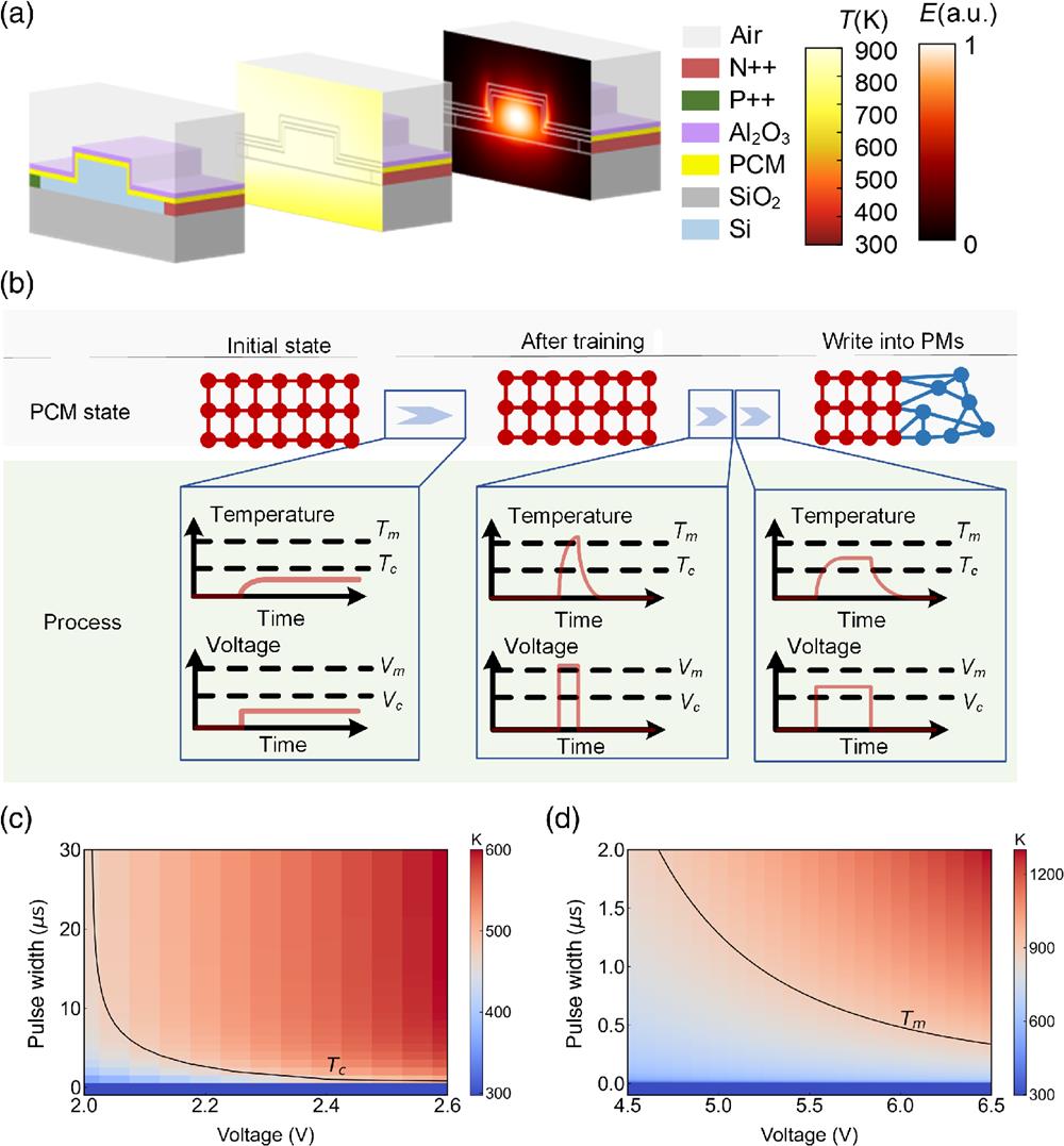
    Fig. 1. Design and operation principle of our PM. (a) Schematic diagram of the PM’s structure, thermal distribution at a 6 V/500 ns voltage pulse, and optical mode profile at 2025 nm, respectively. (b) Operation principle of our PM. Simulated temperature variation of Sb2Se3 patch with applied single pulses of different voltages and durations for (c) crystallization and (d) amorphization.
    Device fabrication and switching performance of our PM. (a) Fabrication flowchart of the device. (b) Microscope image of an Sb2Se3 MRR PM. The inset shows an SEM image of the Sb2Se3 (the shaded region) on top of the PIN diode. (c) Normalized transmittance spectra of the PM after the phase switching between two states of Sb2Se3.
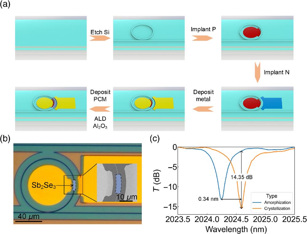
    Fig. 2. Device fabrication and switching performance of our PM. (a) Fabrication flowchart of the device. (b) Microscope image of an Sb2Se3 MRR PM. The inset shows an SEM image of the Sb2Se3 (the shaded region) on top of the PIN diode. (c) Normalized transmittance spectra of the PM after the phase switching between two states of Sb2Se3.
    The change in transmittance of the PM under multilevel states. (a) Amorphization (at 2024.59 nm) and (c) crystallization (at 2024.25 nm). The inset shows the enlarged error bar of two randomly chosen storage levels. Change in the transmittance of the PM with different voltages and pulse widths for (b) amorphization and (d) crystallization.
    Fig. 3. The change in transmittance of the PM under multilevel states. (a) Amorphization (at 2024.59 nm) and (c) crystallization (at 2024.25 nm). The inset shows the enlarged error bar of two randomly chosen storage levels. Change in the transmittance of the PM with different voltages and pulse widths for (b) amorphization and (d) crystallization.
    Volatile modulation of an Sb2Se3 MRR. (a) Normalized transmittance spectra with different forward biases. (b) Dynamic response of the Sb2Se3 MRR.
    Fig. 4. Volatile modulation of an Sb2Se3 MRR. (a) Normalized transmittance spectra with different forward biases. (b) Dynamic response of the Sb2Se3 MRR.
    OCK based on the volatile-modulation-compatible PM. (a) Schematic architecture of a 4×4 OCK. The inset is the solidifying method of the output value of each basic unit in ONNs after on-chip training of OCK. (b) Schematic diagram of the on-chip training and writing operation of the OCK. The accuracy of predictions (c) after the simulated on-chip training of OCK and (d) after simulated writing into PMs.
    Fig. 5. OCK based on the volatile-modulation-compatible PM. (a) Schematic architecture of a 4×4 OCK. The inset is the solidifying method of the output value of each basic unit in ONNs after on-chip training of OCK. (b) Schematic diagram of the on-chip training and writing operation of the OCK. The accuracy of predictions (c) after the simulated on-chip training of OCK and (d) after simulated writing into PMs.
    Maoliang Wei, Junying Li, Zequn Chen, Bo Tang, Zhiqi Jia, Peng Zhang, Kunhao Lei, Kai Xu, Jianghong Wu, Chuyu Zhong, Hui Ma, Yuting Ye, Jialing Jian, Chunlei Sun, Ruonan Liu, Ying Sun, Wei. E. I. Sha, Xiaoyong Hu, Jianyi Yang, Lan Li, Hongtao Lin. Electrically programmable phase-change photonic memory for optical neural networks with nanoseconds in situ training capability[J]. Advanced Photonics, 2023, 5(4): 046004
    Download Citation