
Maoliang Wei, Junying Li, Zequn Chen, Bo Tang, Zhiqi Jia, Peng Zhang, Kunhao Lei, Kai Xu, Jianghong Wu, Chuyu Zhong, Hui Ma, Yuting Ye, Jialing Jian, Chunlei Sun, Ruonan Liu, Ying Sun, Wei. E. I. Sha, Xiaoyong Hu, Jianyi Yang, Lan Li, Hongtao Lin. Electrically programmable phase-change photonic memory for optical neural networks with nanoseconds in situ training capability[J]. Advanced Photonics, 2023, 5(4): 046004
- Advanced Photonics
- Vol. 5, Issue 4, 046004 (2023)
Abstract
Keywords
1 Introduction
In recent years, neural networks based on central processing units (CPUs) have been used in mobile phones for speech recognition and image classification,1 but they are still in their infancy in more sophisticated and expansive application fields where massive amounts of data should be processed in real time, such as autonomous driving2 and computer vision.3 Optical neural networks (ONNs) based on photonic integrated circuits (PICs)4
In on-chip ONNs, weights are determined by basic units of PICs altering their optical phase20 or intensity.21 These basic units commonly employ the thermo-optic (TO) effect, free-carrier dispersion effect, or nano-opto-electromechanical systems,22,23 suffering from severe heat accumulation, high static power consumption or/and large footprint, which constrains the scalability of programmable photonic networks. On-chip integrated photonic memories, which can retain specific optical states after training (referring to all types of training), are anticipated to be embedded in programmable PICs to reduce or even eliminate static power consumption. Chalcogenide phase-change materials (PCMs) are promising candidates for zero static power-consumption photonic memories due to their reversible amorphous-crystalline phase transition,24
On the other hand, in situ training (referring to training the ONN directly in the optical domain) is a potent remedy for enhancing the accuracy of algorithm execution in integrated ONNs,43
Sign up for Advanced Photonics TOC. Get the latest issue of Advanced Photonics delivered right to you!Sign up now
Wavelength division multiplexing (WDM)-based computing is a potential arena for implementing optical CNNs.47 Combined with the nonvolatile modulation of PCM, zero-static power consumption optical CNNs can be achievable.48 Moreover, the combination of WDM and frequency comb makes ONNs with more complex functionality achievable.49 Increasing the number of WDM channels can increase the amount of parallel computation of optical computing. The waveband is a promising candidate for expanding the number of channels thanks to the ignorable two-photon absorption at the waveband of silicon50 and the higher free-carrier dispersion effect of silicon at .51
To date, to the best of our knowledge, nanosecond in situ training-compatible multilevel PM has not yet been studied. Here, we address these challenges by demonstrating an electrically programmable phase-change PM for ONNs. In this work, by integrating a low-loss PCM with a p–i–n (PIN)-diode-embedded micro-ring resonator (MRR), a multilevel PM with more than 5 bits was demonstrated, and any specific intermediate optical state can be configured from an unknown state by applying certain electrical pulses. Meanwhile, volatile modulation with a speed of 15.2 MHz was enabled by keeping the driving voltage of the waveguide-integrated PIN diode under the threshold for triggering the phase change of the PCM. Such photonic memories can simultaneously realize in situ training and data storage in PICs for ONNs. In addition, this work provides a new paradigm for constructing CMOS-compatible, electrically programmable, nonvolatile on-chip photonic accelerators with high-speed in situ training capability, which we believe would contribute to the further development of energy-efficient, large-scale, high-yield ONNs.
2 Device Design
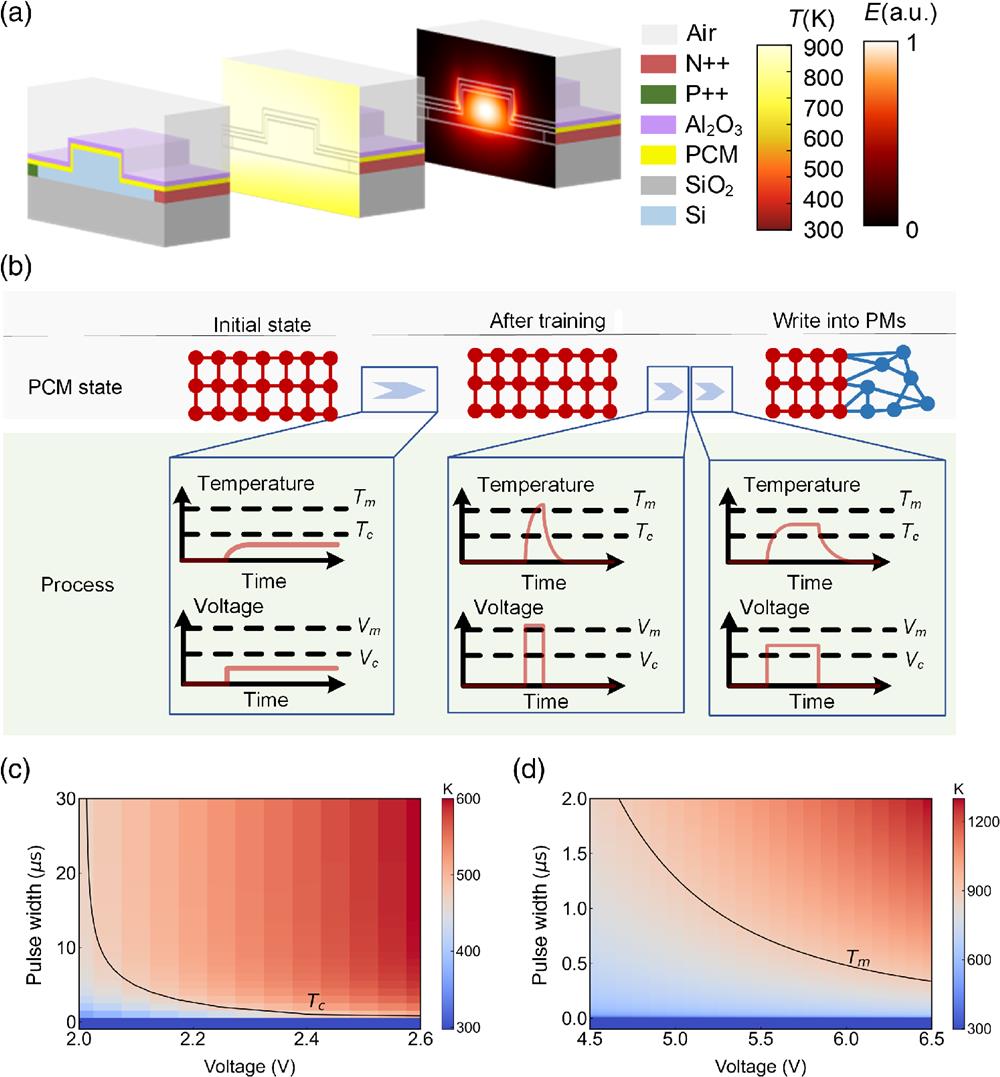
Figure 1(a) shows a schematic diagram of the PM enabling in situ training of ONNs. A patch of phase-change thin film with a thickness of 30 nm was covered on a 600 nm-wide 150 nm-etched silicon waveguide, forming a low-loss hybrid waveguide configuration similar to what we previously demonstrated in Ref. 52. When the phase transition of occurs, it modifies the refractive index of the PCM patch and the effective refractive index () of the hybrid waveguide, which alters the resonant peak of the microring, thus changing the optical output of the PM. A 30 nm-thick film was capped on the top to avoid oxidization of during phase switching. A PIN diode was embedded in the silicon waveguide to not only support fast volatile modulation but also induce phase transition of the PCM above the waveguide by resistive heating.
![]()
Figure 1.Design and operation principle of our PM. (a) Schematic diagram of the PM’s structure, thermal distribution at a 6 V/500 ns voltage pulse, and optical mode profile at 2025 nm, respectively. (b) Operation principle of our PM. Simulated temperature variation of
Figure 1(b) depicts how PCM-integrated photonic memories operate in on-chip ONNs. Before the in situ training began, PCM patches of the photonic memories in an ONN were all initialized to the crystalline state. This was achieved by heating the PCM up via the PIN diode to a temperature higher than its crystallization temperature () and holding for a period of time, for instance, 1 ms. During in situ training, the PIN diode in each PM was driven by a relatively low driving voltage, realizing the free-carrier dispersion effect-based volatile modulating, thus updating the weight in nanoseconds while keeping the temperature of the PCM below its crystallization temperature (). After in situ training, the trained weight information from volatile modulation was written into PCM-integrated memories by the ohmic heating effect of the PIN diode. To realize multibit memory, PCM was melted and then rapidly quenched, further heated to various temperatures between and (melting temperature) to partially crystallize to a certain optical state. After weights are written into PM, the on-chip ONN can compute passively, i.e., maintaining the weight info without power consumption.
The design of the PIN microheater is the key to the PCM-integrated PM. Since we employed standard concentrations of ion implantation in a multiproject wafer (MPW) run offered by the Institute of Microelectronics of the Chinese Academy of Sciences (IMCAS), the distance between the heavily doping area and waveguide core was designed to balance the insertion loss and heating efficiency. The propagation loss of our PIN-diode-embedded waveguide is simulated to be and experimentally measured to be (see Sec. S1 in the Supplementary Material). Figure 1(a) shows the distribution of the thermal field in the PM when a 6 V/500 ns voltage pulse is applied. It could be seen that the PIN diode can effectively heat the PCM up to a certain temperature and induce a corresponding phase change by applying specific electrical pulses.
To separately manipulate volatile modulation and nonvolatile storage, electric pulses needed to be studied. According to our simulation, the bias current applied for fast volatile modulation based on the free-carrier dispersion effect should be lower than 5.84 mA to avoid the TO effect (see Sec. S2 in the Supplementary Material). At this point, the temperature of the whole waveguide region was simulated to be lower than 355 K, far below the crystallization temperature of .
To write data to the PM, the driving voltage and pulse duration are the main parameters that need to be carefully designed and optimized. The longest pulse duration (or switching speed) of a PCM-based PM is limited by the crystallization process. Figure 1(c) shows the crystallization temperature of an patch on the PIN diode with applied single pulses of different voltages and durations. It could be seen that the pulse duration needed for crystallization could be shortened by appropriately increasing the driving voltage, considering that the driving voltage required for crystallization is relatively low. In contrast, the highest driving voltage needed for a PCM-based PM depends on the amorphization process due to higher than , as shown in Fig. 1(d). However, the voltage of the amorphization pulse cannot be arbitrarily lowered by prolonging the pulse duration. On the one hand, the thermal decay rate of the system has to be larger than the critical cooling rate53 to avoid recrystallization, yet the thermal decay time of the system is simulated to increase with the prolonged pulse duration. On the other hand, continuous increasing of the pulse duration with a certain voltage amplitude ultimately leads to thermal saturation, and an overlong pulse duration brings about limited benefits. Hence, the duration of amorphization pulses is limited to within in our design. It could be seen from Fig. 1(d) that the driving voltage could be optimized down to 5 V theoretically. This driving voltage could be supplied by integrated circuits in standard CMOS technologies.54
Therefore, this PCM-integrated PM could potentially achieve a nonvolatile write speed of microseconds and write voltage lower than 5 V, as well as volatile modulation with nanoseconds for in situ training for ONNs. Although the optical loss in volatile phase modulation of a PIN diode is higher than that of a p–i–p (PIP) or n–i–n (NIN) doping waveguide,55,56 it has prominent advantages of higher speed for volatile modulation due to the usage of the free-carrier dispersion effect of silicon rather than the TO effect of silicon. Moreover, the optical loss induced during volatile modulation becomes exploitable by integrating such a design with an MRR. Finally, the PIN diode microheater can reduce the driving voltage needed for phase switching of PCM compared to the PIP or NIN doping profile.31,40
3 Multibit Low-Loss Photonic Memory
We experimentally demonstrated the -integrated PM in the form of an all-pass MRR ( MRR). Figure 2(a) shows a schematic diagram of the fabrication process. The waveguide patterning and ion implantation were performed in an MPW run offered by IMCAS. The doping concentrations of p-type and n-type were and , respectively. Then, metallic electrodes (5 nm Cr/100 nm Au) and patches were fabricated by UV lithography followed by a lift-off process. Finally, a 30 nm was deposited, and the metal contact window was opened by etching.
![]()
Figure 2.Device fabrication and switching performance of our PM. (a) Fabrication flowchart of the device. (b) Microscope image of an
Figure 2(b) shows an optical microscope image of the fabricated MRR with a radius of . A -long patch was covered on a -long PIN diode embedded in the resonator. A home-built integrated photonic measurement setup (see Sec. S3 in the Supplementary Material) was used to characterize the PM. To eliminate the temperature perturbation derived from ambient temperature variation, the temperature of the substrate of the photonic chip is held to 30°C throughout the test via a temperature control system. Figure 2(c) shows the change of normalized transmittance () spectra of the MRR when the phase transition of occurs. When was crystallized by a 3.0 V/1 ms voltage pulse or amorphized by an 8.2 V/500 ns pulse, a resonance peak shift of 0.34 nm and an extinction ratio over 14 dB were realized.
Here, we systematically characterized the effect of amplitude and duration of voltage pulses on the multilevel switching response of photonic memories. The patch was gradually amorphized and generated 38 levels in the PM by applying an electric pulse with a duration of 500 ns and voltage amplitudes not exceeding 8.2 V. The transmission change () and storage levels are shown in Fig. 3(a). Each optical storage level is the average value of 50 measurements in the same state to avoid test errors due to systematic noise. The lowest resolution of these memory states is 0.07 dB. Among them, 28 levels were distinguishable after the transmission change is converted to the linear region, which can be used for info storage for optical computing. As our simulations confirmed, prolonging the pulse width can reduce the driving voltage for the melt quenching of during amorphization [see Fig. 3(b)]. By employing a pulse duration of , the driving voltage needed for partial amorphization of to generate a transmittance change could be reduced to 5.3 V. The device would be damaged once the pulse duration of the relatively high-voltage amorphization pulse exceeded ; hence, the pulse duration should be kept within . The amorphization driving voltage could be reduced to 4.4 V by narrowing the gap between the waveguide and the metal contact (see Sec. S4 in the Supplementary Material), suggesting good scaling potential with improved energy efficiency.
![]()
Figure 3.The change in transmittance of the PM under multilevel states. (a) Amorphization (at 2024.59 nm) and (c) crystallization (at 2024.25 nm). The inset shows the enlarged error bar of two randomly chosen storage levels. Change in the transmittance of the PM with different voltages and pulse widths for (b) amorphization and (d) crystallization.
As for multilevel crystallization, by applying fixed voltage amplitude at 3 V and various pulse durations of no more than , 40 memory states were demonstrated with a resolution higher than 0.07 dB, as shown in Fig. 3(c). After conversion to the linear domain, there are still 34 different states (more than 5 bits). Each level was also averaged by 50 measurements. The standard deviation in Fig. 3(c) confirms that the states are separable even with noise in the measurement system. The write speed of the PM could be further improved by increasing the driving voltage for crystallization, as shown in Fig. 3(d), consistent with our design.
Hence, a 5-bit PCM-integrated PM was demonstrated, with a driving voltage lower than 10 V and a switching time within tens of microseconds. The experimental driving voltage is not as low as the simulated one, which may result from nonideal ion implantation and activation in the device fabrication.
4 Volatile Modulation-Compatible Photonic Memory for ONNs
A photonic neural network with PCM-integrated memory is of zero static power consumption, but in situ training via continually and intensively switching the phase of PCM is neither energy-efficient nor fast enough. Here, we address this issue by embedding a volatile modulation function into nonvolatile PM. Figure 4(a) shows the change of normalized transmittance spectra of the PM during volatile modulation used in the in situ training process. Note that the patch on the PIN diode is now amorphized. The ripples of the measured spectra resulted from the Fabry–Perot resonance due to the reflection of the grating coupler. A peak shift efficiency of was realized. Figure 4(b) shows the dynamic response of the PM when a 1.3 V, 1 MHz square-wave signal was applied. The 10%-to-90% rising time () and 90%-to-10% falling time () are characterized to be 13.4 and 23.0 ns, respectively, corresponding to a 3 dB bandwidth of 15.2 MHz.
![]()
Figure 4.Volatile modulation of an
Here, we simulated electrically programmable ONNs by Python exemplified by a optical convolution kernel (OCK) constructed by the PM, as shown in Fig. 5(a). Since the PCM-integrated PM was demonstrated in the form of an MRR, the convolution operation was implemented through a WDM scheme. Modulated optical signals with four different wavelengths were equally sent to the OCK in four equal channels. After the optical convolution operation, optical signals were converted to electrical signals, amplified by the transimpedance amplifier, and then processed by the CPU. Any intermediate storage state could be configured from an unknown state by employing two electrical pulses (one for amorphization and the other for crystallization), and the measured transmission change () is shown in the inset of Fig. 5(a). Thus, our proposed OCK is capable of both fast on-chip training and computing with near-zero power consumption.
![]()
Figure 5.OCK based on the volatile-modulation-compatible PM. (a) Schematic architecture of a
The PM-embedded OCK was theoretically verified by the MNIST handwritten digit database. Before the on-chip training of OCK execution, the states of all SbSe patches are initialized to their crystalline state. After that, the on-chip training of OCK was implemented by exploiting the volatile modulation of our PM. Then, the trained weights were written to the PM by applying a reset (amorphization) pulse followed by a fractional-crystallization pulse after the on-chip training of OCK. Figure 5(b) shows a schematic diagram of the evolution of measured transmittance spectra and kernel value. The trained and stored MRR arrays have different transmittance spectra, since the on-chip training of OCK and writing were conducted through different principles and approaches. Yet the value of weights after the on-chip training of OCK and writing should be as close as possible (and ideally the same). The question naturally arises over whether the discrete storage states of PCM-based PMs may lead to performance deterioration of the OCK. To verify this, the accuracy of predictions after the simulation of the on-chip training of OCK via PIN diodes () is shown in Fig. 5(c). After the trained parameters were written into the PMs, the implementation of the network reached minimal deviation in accuracy, as shown in Fig. 5(d). Note that the scale of the MRR array could be easily expanded. Considering there are channels for data processing, the OCK could be scaled up to by simply decreasing the radius of the MRR to in theory (see Sec. S5 in the Supplementary Material).
The PM-based convolution core benefits both on-chip training of OCK and low-static power computing. The on-chip training of OCK based on the volatile-compatible PM provides a training speed typically 1000 times faster than the commonly used TO scheme.20 After on-chip training of OCK, the computing is done passively without static power consumption. With this scheme, the saved power consumption of an OCK is , compared with the typical TO modulator array with 10 mW of each discrete device on average.20,57 Therefore, the ONNs with PM are attractive in sporadic programming applications, and the power efficiency would increase with the scaling up of PICs.
In large-scale ONNs where PMs are expected to be used in the whole linear network, multibit storage of PMs can play a significant role. For instance, constructing an ONN (with a OCK) from PMs where the in situ training results showed an averaged prediction accuracy rate of 94.64% identifying the MNIST data set, PMs need at least 4 bits to achieve comparable prediction accuracy (averaged accuracy rate ), as shown in Sec. S6 in the Supplementary Material. This indicates that multibit PMs are necessary for high-performance ONNs, and higher bits are expected for more complicated applications.
5 Conclusion
In this work, we proposed an electrically programmable phase-change PM for energy-efficient in situ training ONNs with CMOS compatibility and scalability. By integrating an phase-change patch onto a PIN diode, we designed and experimentally validated the PCM-driven 5-bit PM using an MRR. The PM exhibits a transmittance contrast of , creating 28/34 storage levels during amorphization/crystallization, and the corresponding pulse voltages (pulse durations) are 7.4 to 8.2 V ()/3 V (10 to ). Furthermore, theoretically, complete amorphization of can be induced by a 500-ns electrical pulse with an actuation voltage as low as 3.3 V, which can be provided by an integrated circuit with standard CMOS technology. In our experiment, fractional amorphization was achieved by applying a voltage pulse. Volatile modulation with a bandwidth of was also achieved in this PM when electric pulses with voltages lower than 2 V were applied, enabling a 1000 times faster training in theory for nonvolatile ONNs composed of such PMs than the commonly used TO switches. After training, PMs are configured to specific states via PIN-microheater-assisted multilevel switching (i.e., partial phase transition) of to match the target weight values in the ONNs. According to our simulations, at least 4 bits are needed for PMs to maintain the accuracy of predictions of ONNs after the simulated in situ training when tested by the MNIST handwritten data set. This study on volatile modulation-compatible PM provides a feasible solution for constructing nonvolatile ONNs with high-speed and energy-efficient on-chip training capability.
Maoliang Wei is a doctoral candidate student of Professor Hongtao Lin at Zhejiang University. He received his BS degree in electronic information science and technology from Xiamen University. His current research focuses on the study of micronano devices and systems.
Junying Li is an associate professor at the College of Information Science and Electronic Engineering, Zhejiang University, Hangzhou, Zhejiang, China. She received her BS and PhD degrees from Chongqing University, Chongqing, China. Her research is focused on chalcogenide phase-change materials, reconfigurable photonic devices, and their applications.
Hongtao Lin is a ZJU100 Young Professor at the College of Information Science and Electronic Engineering, Zhejiang University, Hangzhou, Zhejiang, China. He received his BS degree from the University of Science and Technology of China, Hefei, China, and his PhD from the University of Delaware, Newark, Delaware, USA. His research interests are focused on chalcogenide integrated nanophotonics and their applications.
Biographies of the other authors are not available.
References
[11] W. Bogaerts et al. Programmable photonic circuits. Nature, 586, 207-216(2020).
[13] H. Shu et al. Microcomb-driven silicon photonic systems. Nature, 605, 457-463(2022).
[14] S. Bandyopadhyay et al. Single chip photonic deep neural network with accelerated training(2022).
[21] Z. G. Cheng et al. On-chip photonic synapse. Sci. Adv., 3, e1700160(2017).
[32] C. Ríos et al. In-memory computing on a photonic platform. Sci. Adv., 5, eaau5759(2019).
[42] X. Ma et al. Photonic tensor core with photonic compute-in-memory, 1-3(2022).
[46] S. M. Buckley et al. Photonic online learning: a perspective. Nanophotonics, 12, 833-845(2023).
[49] B. Bai et al. Microcomb-based integrated photonic processing unit. Nat. Commun., 14, 66(2023).
[50] R. Soref. Mid-infrared photonics in silicon and germanium. Nat. Photonics, 4, 495-497(2010).
[54] H. Ballan, M. Declercq. High Voltage Devices and Circuits in Standard CMOS Technologies, 268-269(2013).

Set citation alerts for the article
Please enter your email address
© Copyright 2018-2021 | Chinese Laser Press. All Rights Reserved 沪ICP备15018463号-20