• Chinese Optics Letters
  • Vol. 16, Issue 2, 020006 (2018)
You Zheng, Changyong Lan, Zhifei Zhou, Xiaoying Hu, Tianying He, and Chun Li*
Author Affiliations
  • State Key Laboratory of Electronic Thin Films and Integrated Devices, and School of Optoelectronic Information, University of Electronic Science and Technology of China, Chengdu 610054, China
  • show less
    DOI: 10.3788/COL201816.020006 Cite this Article Set citation alerts
    You Zheng, Changyong Lan, Zhifei Zhou, Xiaoying Hu, Tianying He, Chun Li. Layer-number determination of two-dimensional materials by optical characterization[J]. Chinese Optics Letters, 2018, 16(2): 020006 Copy Citation Text show less
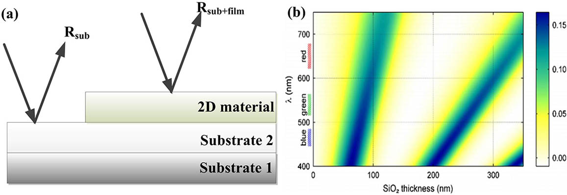
    (a) Schematic of the optical contrast definition. (b) A color plot of the contrast as a function of the wavelength and the SiO2 thickness[14].
    Fig. 1. (a) Schematic of the optical contrast definition. (b) A color plot of the contrast as a function of the wavelength and the SiO2 thickness[14].
    (a) Contrast spectra of graphene with different LNs on 300 nm SiO2 substrate. (b) The optical images of all the samples in (a). The graphene flakes in a, b, c, d, e, and f are more than 10 layers and the thickness increases from a to f[19].
    Fig. 2. (a) Contrast spectra of graphene with different LNs on 300 nm SiO2 substrate. (b) The optical images of all the samples in (a). The graphene flakes in a, b, c, d, e, and f are more than 10 layers and the thickness increases from a to f[19].
    The G and 2D modes of graphene vary with different layers[27].
    Fig. 3. The G and 2D modes of graphene vary with different layers[27].
    (a) Four active Raman modes in bulk MoS2. (b) Raman spectra of atomically thin and bulk MoS2 films. (c) The frequency shifts of two characteristic Raman modes and their difference as a function of LNs[29].
    Fig. 4. (a) Four active Raman modes in bulk MoS2. (b) Raman spectra of atomically thin and bulk MoS2 films. (c) The frequency shifts of two characteristic Raman modes and their difference as a function of LNs[29].
    (a) Raman spectra of BP with different numbers of layers. (b) The schematic structural view of monolayer BP showing the crystal orientation. (c) The polarization-resolved Raman scattering spectra of monolayer BP with linearly polarized laser excitation. (d) The intensity of the Ag1 mode as a function of the laser polarization angle in the x-y plane[33].
    Fig. 5. (a) Raman spectra of BP with different numbers of layers. (b) The schematic structural view of monolayer BP showing the crystal orientation. (c) The polarization-resolved Raman scattering spectra of monolayer BP with linearly polarized laser excitation. (d) The intensity of the Ag1 mode as a function of the laser polarization angle in the x-y plane[33].
    Calculated band structure of (a) bulk, (b) quadrilayer, (c) bilayer, and (d) monolayer MoS2[37].
    Fig. 6. Calculated band structure of (a) bulk, (b) quadrilayer, (c) bilayer, and (d) monolayer MoS2[37].
    (a) PL spectra of monolayer and bilayer MoS2. (b) The normalized PL spectra of MoS2 with increasing LNs (c) The evolution of the bandgap with increasing MoS2 LNs[29].
    Fig. 7. (a) PL spectra of monolayer and bilayer MoS2. (b) The normalized PL spectra of MoS2 with increasing LNs (c) The evolution of the bandgap with increasing MoS2 LNs[29].
    SHG of (a) MoS2 and (b) h-BN with different layers[43].
    Fig. 8. SHG of (a) MoS2 and (b) h-BN with different layers[43].
    (a) Optical micrograph of MoS2. (b) The SHG and (c) the THG images with few-layer areas under 1560 nm excitation. (d) The intensity of the SHG and THG as a function of LNs[47].
    Fig. 9. (a) Optical micrograph of MoS2. (b) The SHG and (c) the THG images with few-layer areas under 1560 nm excitation. (d) The intensity of the SHG and THG as a function of LNs[47].
    ReferenceStructureMaterialMax Theoretical Contrast
    [14]Film/SiO2/SiGraphene15%  @  560 nm
    [21]Film/SiO2/Si, film/glassGraphene10% @  570 nm
    [22]Film/Si3N4/SiGraphene oxide80% @ 550nm*
    [16]PMMA/film/SiO2, Si3N4, Al2O3, TiO2, Si, Ge, GaAs, ZnO, Au, Cu, etc.Graphene59.73% @ 400 nm (HfO2)*
    [23]Film/72 nm Al2O3/SiGraphene12% @ 450 nm
    [12]Film/SiO2/SiMoS2, WSe2, NbSe280%, 45%, 40% (495–530 nm)
    [17]Film/75 nm Si3N4/SiMoS2, MoSe2, WSe2, BP45% @ 550 nm (MoS2)
    [20]Film/SiO2/Ag/SiGraphene10% (500–700 nm)
    [24]SiO2/film/SiO2/SiGraphene, MoS2, WS2, WSe2, MoS270% (MoS2 500–560 nm)
    Table 1. Recently Reported Structures for Enhancing Optical Contrast
    You Zheng, Changyong Lan, Zhifei Zhou, Xiaoying Hu, Tianying He, Chun Li. Layer-number determination of two-dimensional materials by optical characterization[J]. Chinese Optics Letters, 2018, 16(2): 020006
    Download Citation