Abstract
Initiated by graphene, two-dimensional (2D) layered materials have attracted much attention owing to their novel layer-number-dependent physical and chemical properties. To fully utilize those properties, a fast and accurate determination of their layer number is the priority. Compared with conventional structural characterization tools, including atomic force microscopy, scanning electron microscopy, and transmission electron microscopy, the optical characterization methods such as optical contrast, Raman spectroscopy, photoluminescence, multiphoton imaging, and hyperspectral imaging have the distinctive advantages of a high-throughput and nondestructive examination. Here, taking the most studied 2D materials like graphene, , and black phosphorus as examples, we summarize the principles and applications of those optical characterization methods. The comparison of those methods may help us to select proper ones in a cost-effective way.Micromechanical exfoliated graphene opened the research field of two-dimensional (2D) materials. Since then, more and more 2D layered materials, including molybdenum sulfide (), hexagonal boron nitride (h-BN), black phosphorus (BP), and so on, have been reported and have attracted great interest. Compared with conventional electronic and optical materials, 2D materials show many unique properties such as record-high charge carrier mobility, strong light–matter interaction, and superior mechanical properties[1–3], which implies promising applications for novel devices[4]. However, many of those fascinating properties are strongly dependent on their layer numbers (LNs). For example, monolayer graphene has a zero bandgap, while bilayer graphene on SiC substrate has a finite bandgap of [5]. Monolayer is a direct bandgap semiconductor, but bilayer is an indirect one. While the bandgap of BP decreases as the number of layers increases from monolayer (1.5–2.0 eV) to bulk (0.2 eV)[6]. In addition, at present, it is still a great challenge to precisely control the LN of 2D materials in large scale, although there are many methods for preparing 2D materials including micromechanical exfoliation[7], epitaxial growth[8], chemical vapor deposition (CVD)[9], and liquid phase exfoliation[10]. Therefore, it is critical to find an efficient and reliable way to identify their LNs, which is important for both fundamental research and industrial application.
Among the numerous thickness characterization methods, atomic force microscopy (AFM), scanning electron microscopy (SEM), and transmission electron microscopy (TEM) are the most intuitive approaches. Nevertheless, these structural characterization methods are usually low in throughput, prone to sample damage, and strict with substrate choosing. For example, during the measuring process of AFM in contact mode, the cantilever tip always needs contacting with the sample, which may cause irreversible physical damage to the samples. In the SEM observation, conductive substrates are required to eliminate the charge accumulation. The low-voltage mode is much sensitive to small surface features but decreases the signal-to-noise ratio. The TEM characterization requires sophisticated skills and experiences with sample preparation. For optical characterization, due to the strong LN-dependent light–matter interactions of 2D materials, the variation of optical signals collecting from the scattering, absorption, or light emission can be correlated to the LNs. Therefore, by detecting these optical signals and interpreting their peak position, intensity, and line shape associated with LNs, their exact LNs can be accurately determined. Such an optical characterization is nondestructive, with high throughput, and reliable. Here, we review the principles and recent development of the commonly adopted optical characterization methods, and compare their advantages and limitations.
This review is organized as follows. After the introduction, we first focus on the most frequently used method, the reflective optical contrast, to identify the LNs of 2D materials laying on nontransparent substrates. Particularly, we summarize the reported strategies on improving the visibility of 2D materials by engineering the reflection contrast of the substrates. Then, Raman and photoluminescence (PL) characterizations of typical 2D materials (graphene, , and BP) are briefly reviewed. The multiphoton spectrum relying on nonlinear absorption is one of the focuses in another section. Other methods mainly regarding the identification of 2D materials on transparent substrate are also discussed. Finally, we present a summary and an outlook for the research field. We note that during our preparation of this review, another comprehensive review paper mainly focusing on Raman characterization was published[11], which is also a valuable reference for the optical characterization of 2D materials.
Sign up for Chinese Optics Letters TOC. Get the latest issue of Chinese Optics Letters delivered right to you!Sign up now
Undoubtedly, reflective optical contrast is the most direct and convenient method to identify the LNs of 2D materials, and is especially useful for finding monolayer microflakes from the micromechanical exfoliated samples in checking under microscopy[12]. Owing to their ultrathin features, the optical transmittances are very high ( for monolayer graphene), making them generally invisible on most substrates. Thanks to a special substrate of Si wafer capped with a 300 nm , monolayer graphene can be vividly seen by the naked eye[13]. A more clear contrast image can be obtained by observing the sample under conventional reflective optical microscopy. This simple and effective technique of direct visualization of atomically thin materials not only makes the great success of graphene, but also offers a quick way to identify other monolayer materials, which greatly accelerates the exploration of new 2D materials.
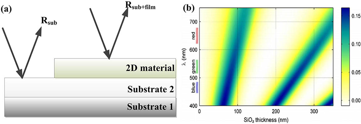
To explain this amazing phenomenon, Blake et al.[14] first proposed a strict calculation using the Fresnel principle. When light is incident from air onto a 2D material laying on a dielectric substrate, multiple reflections at the interfaces occur and optical interference within the medium of multilayer structure will modify the intensity of reflection from 2D material. As shown in Fig. 1(a), the optical contrast is defined as the difference between the light reflection intensity from the 2D materials deposited on substrate and that from the bare substrate. The calculating formula can be written by , where and represent the reflectance of substrate and 2D materials, respectively. Via well-established recursive[15] and transfer matrix methods[16–18], both of which are derived from the Fresnel principle, this enhancement effect can be theoretically calculated and found to be well matched with the experimental results[19]. As shown in Fig. 1(b), the calculation result shows that the optical contrast of monolayer graphene on has two visualization channels. One is for and the other is for with a slightly wider range. Note that a near 10% optical contrast around 550 nm is enough for direct eye recognition. Figure 2(a) shows the contrast spectra of different graphene layers on the 300 nm substrate. The corresponding optical images of the samples are shown in Fig. 2(b)[19]. As can be seen, with LN increasing, the contrast clearly consistently increases.
![(a) Schematic of the optical contrast definition. (b) A color plot of the contrast as a function of the wavelength and the SiO2 thickness[14].](/Images/icon/loading.gif)
Figure 1.(a) Schematic of the optical contrast definition. (b) A color plot of the contrast as a function of the wavelength and the thickness[14].
Figure 2.(a) Contrast spectra of graphene with different LNs on 300 nm substrate. (b) The optical images of all the samples in (a). The graphene flakes in a, b, c, d, e, and f are more than 10 layers and the thickness increases from a to f[19].
This method is also found very effective for other 2D materials. To maximize the reflection contrast for easier distinction, many structures of the substrates have been proposed. For example, Lee et al.[20] proposed that a structure of Ag film covered with 81 nm as the light cavity also shows optical contrast with a much broader range than that of conventional 300 nm substrate. Teo et al.[16] have theoretically studied the visibility of graphene on different types of substrates, including metals, semiconductors, and insulators. They found that by coating a polymethylmethacrylate (PMMA) layer on the graphene/dielectric substrate the contrast can be further improved. Table 1 summarizes the recently reported structures for enhancing optical contrast on nontransparent substrates. Obviously, the maximum contrast is strongly wavelength dependent. Therefore, a narrow bandpass filter is typically required to improve the contrast.
| Reference | Structure | Material | Max Theoretical Contrast |
|---|
| [14] | Film/SiO2/Si | Graphene | ∼ 15% @ 560 nm |
| [21] | Film/SiO2/Si, film/glass | Graphene | ∼10% @ 570 nm |
| [22] | Film/Si3N4/Si | Graphene oxide | ∼ 80% @ 550 nm* |
| [16] | PMMA/film/SiO2, Si3N4, Al2O3, TiO2, Si, Ge, GaAs, ZnO, Au, Cu, etc. | Graphene | 59.73% @ 400 nm (HfO2)* |
| [23] | Film/72 nm Al2O3/Si | Graphene | ∼ 12% @ 450 nm |
| [12] | Film/SiO2/Si | MoS2, WSe2, NbSe2 | ∼ 80%, ∼ 45%, ∼ 40% (495–530 nm) |
| [17] | Film/75 nm Si3N4/Si | MoS2, MoSe2, WSe2, BP | ∼ 45% @ 550 nm (MoS2) |
| [20] | Film/SiO2/Ag/Si | Graphene | ∼ 10% (500–700 nm) |
| [24] | SiO2/film/SiO2/Si | Graphene, MoS2, WS2, WSe2, MoS2 | 70% (MoS2 500–560 nm) |
Table 1. Recently Reported Structures for Enhancing Optical Contrast
It is worth mentioning that reflective optical contrast is a very efficient method to identify monolayer 2D materials on the above-mentioned reflectively enhanced substrates. However, to quantitatively determine the LN by this method, one needs to measure the reflection spectra and fit them with the calibrated LN-dependent reflection of the same material on the same substrate. It also should be noted that finding monolayer by contrast is experience dependent. Without careful training on the comparison of the calibrated LN-related contrast images, it is difficult to give an accurate assignment of the LNs.
Raman is also a powerful tool for counting the LNs of 2D materials. Because of highly LN sensitive lattice vibration and phonon dispersion of 2D materials, the LNs of the sample can be precisely determined by detecting the variation of intensity, peak position, and line shape of the characteristic Raman peaks[25]. Raman spectroscopy was first applied for characterizing the LN of graphene. In graphene, there are two characteristic Raman modes, mode and mode, whose line shape and intensity are important for identifying the LNs. The band originates from the in-plane vibration of carbon atoms and is a doubly degenerate (TO and LO) photon mode ( symmetry) at the Brillouin zone center[26]. The band originates from a two-phonon double resonance Raman process. Because the interlayer coupling is much weaker than the intralayer C-C bonding, the interlayer coupling almost does not affect the C-C bonding in multilayer graphene. Therefore, it is revealed that the peak position of the mode is not sensitive to LN[11]. As shown in Fig. 3, except for the increase in the intensity, the position and line shape of mode do not change with the increase of LNs, while the line shape of the mode exhibits strong dependence on LNs[27]. The observed layer-dependent characteristics of the peak could, in principle, be attributed to the splitting of the phonon branches or the splitting of the electric band with increasing LNs. The intensity ratio of the mode to the mode can also be used to determine the LNs of graphene. Generally, is greater than 2 for a high-quality monolayer graphene[28].
Figure 3.The and modes of graphene vary with different layers[27].
For transition metal dichalcogenides (TMDCs), Mak et al.[29], have systematically investigated the layer-dependent Raman spectra of . Figure 4(a) presents four Raman-active modes existing in a bulk sample. Usually, and modes, standing for in-plane and out-of-plane vibration, respectively, can be observed. The absence of the other two modes is attributed to the selection rules associated with scattering geometry. All film thicknesses in Fig. 4(b) have strong signals from both in-plane and out-of-plane . When the LN increases, the out-of-plane atom vibration in is suppressed by the interlayer van der Waals force, resulting in higher force constants[30]. Thus, mode has a blueshift. Different from mode, the mode has a redshift, which is believed to be affected by the long-range interlayer Coulomb interaction between Mo atoms. Moreover, with increasing LN, the intensities of the two modes are both stiffened. Figure 4(c) displays the peak position evolution of and modes with different LNs. By analyzing the difference between these two modes, the LN can be determined.
Figure 4.(a) Four active Raman modes in bulk . (b) Raman spectra of atomically thin and bulk films. (c) The frequency shifts of two characteristic Raman modes and their difference as a function of LNs[29].
For BP, its Raman spectroscopy mainly consists of three characteristic Raman peaks , , and , as shown in Fig. 5(a). The frequency shift between and is regarded as a criterion of the LN[31]. From bulk to bilayer BP, the frequency shift changes from 28 to , and in monolayer BP, the difference between the two peaks is . Utilizing this layer-dependent characteristic of these two peaks, it is possible to rapidly identify single and bilayer BP samples. In addition, different from highly symmetric 2D materials like graphene, BP is an anisotropic material whose lattice orientation can be reflected by Raman spectroscopy. The Raman intensities of , , and modes in BP show an obvious periodic variation with the sample rotation angle under both parallel and cross-polarization configurations[32]. As shown in Figs. 5(c) and 5(d), when the polarization direction of the incident laser is parallel to the zigzag lattice orientation, the intensity of and peaks will reach their maximum. However, when the polarization direction of the incident laser is perpendicular to the zigzag lattice orientation or parallel to the armchair lattice orientation, the intensity of the peak still reaches its maximum, while the peak decreases to a minimum value[33].
Figure 5.(a) Raman spectra of BP with different numbers of layers. (b) The schematic structural view of monolayer BP showing the crystal orientation. (c) The polarization-resolved Raman scattering spectra of monolayer BP with linearly polarized laser excitation. (d) The intensity of the mode as a function of the laser polarization angle in the plane[33].
Compared with the optical contrast technique, Raman spectroscopy is a more quantitative way to determine the LNs of 2D materials. However, accurate LN determination is only effective for few-layer samples. For example, as shown in Fig. 4(c), when the LN of increases to 6, the wavenumber difference between two characteristic modes starts converging to the bulk values. Therefore, a reliable Raman-sensitive LN of is 5[34]. For graphene, this value is about 10. In addition, combined with the mapping technique, it is versatile to give the LN distribution of the sample[35].
In stark contrast to gapless graphene, 2D semiconductors have finite gaps. Due to strong quantum confinement, the band structures strongly depend on their thickness. The typical examples are TMDC materials whose bandgaps are mostly in the visible range. By using the density functional theory[36], the band structures of monolayer, bilayer, quadrilayer, and bulk are calculated as shown in Fig. 6. It can be seen that the direct transition of monolayer occurs at the Brillouin zone K point, and the indirect transition of multilayer occurs between the lowest point of the conduction band and the highest point of the valence band. What’s more, bulk has an indirect bandgap about 1.3 eV, with no obvious fluorescence effect. But when thinned down to a monolayer, it becomes a direct bandgap material, implying a much higher quantum efficiency of PL[29], as shown in Fig. 7(a). This is because multilayer is an indirect bandgap semiconductor whose electronic transitions need not only energy but also the absorption of phonons to change momentum. Generally, in order to characterize the variations in thickness, a normalized processing for PL intensity is performed, as shown in Fig. 7(b). , peaks are two characteristic peaks that correspond to two kinds of excitons. Figure 7(c) shows the homologous variation of the bandgap for 2–6 layers ; the indirect bandgap shifts to lower energies, approaching the indirect bandgap of 1.29 eV with increasing LNs.
Figure 6.Calculated band structure of (a) bulk, (b) quadrilayer, (c) bilayer, and (d) monolayer [37].
Figure 7.(a) PL spectra of monolayer and bilayer . (b) The normalized PL spectra of with increasing LNs (c) The evolution of the bandgap with increasing LNs[29].
By virtue of the high sensitivity of the CCD detector, the visible-range PL emission can be directly recorded without a relatively time-consuming mapping technique, which is very useful for distinguishing the monolayer region. In the most practical cases, optical contrast, Raman and PL are combined to give an accurate characterization of the thickness[38].
Multiphoton imaging is carried out based on the nonlinear optical effect in 2D materials. Generally, one atom or molecule only absorbs one photon when excited from ground state to a high energy state. However, when the light intensity is high enough, one atom or molecule could undergo multiphoton transitions. In other words, it can absorb multiple photons at a time. Taking second-harmonic generation (SHG) as an example, photons with the same frequency interacting with a nonlinear material are effectively combined to generate new photons with twice the energy, and therefore twice the frequency and half the wavelength of the initial photons. It has been proved that 2D materials have remarkable nonlinear properties such as large nonlinear refractive index, huge two-photon absorption, and significant third-order nonlinear susceptibility[39–41]. As reported, the nonlinear refractive index of graphene is as high as , which is about 9 orders of magnitude higher than that of ordinary bulk dielectric materials under the radiation of a 1550 nm fiber laser[42]. By detecting or imaging the harmonic signals generated from light–matter interaction, the microstructure, thickness, and orientation of the sample can be acquired.
The SHG of materials is coherent. In other words, when the radiation of a nonlinear medium is in phase, interference happens, leading to the increase of harmonic intensity; when the radiation phase mismatches, the harmonic intensity decreases to zero owing to destructive interference. Because of the asymmetric structure of odd and h-BN, the SHG can be clearly observed. Figures 8(a) and 8(b) show the second harmonic intensity of and h-BN, respectively. When the LN is odd, the SHG signals decrease with the increase of . However, for samples with even layers, the signals from adjacent layers would cancel each other, leading to very weak response[43].
Figure 8.SHG of (a) and (b) h-BN with different layers[43].
Although the SHG can distinguish the parity of LNs, it can not characterize the change of even layers. Recently, the multiharmonic imaging technique has been proposed to solve this problem[44–46]. Säynätjoki et al.[47] made a comparison between the second and third harmonic generation (THG) for detecting the LNs of . By low-energy continuum-model Hamiltonians[48] and the finite temperature many-body diagrammatic perturbation theory[49], the intensity can be calculated. The results show that the intensity of THG is one order of magnitude larger than that of SHG. Figure 9(a) is the optical micrograph of a micro-exfoliated sample. Figures 9(b) and 9(c) are the SHG and THG images under 1560 nm excitation. Figure 9(d) represents the dependence of the intensity of THG on LNs. As shown in Fig. 9, compared to the SHG, the discrimination of the THG image is significantly enhanced. However, according to the formula derived from Maxwell’s formulas for a nonlinear medium, the THG signal starts to saturate for [47].
Figure 9.(a) Optical micrograph of . (b) The SHG and (c) the THG images with few-layer areas under 1560 nm excitation. (d) The intensity of the SHG and THG as a function of LNs[47].
Remarkably, except for characterizing the LNs, multiphoton imaging is also an efficient way to visualize the grain boundary. Particularly, in contrast to Raman and PL imaging, THG microscopy provides excellent sensitivity in distinguishing grain boundaries, even for samples with small axis rotation between the adjacent grain boundaries[50].
In addition to the above-mentioned generally applied characterization techniques, many novel techniques, such as interference reflection[51] and hyperspectral imaging, have been developed. Interference reflection imaging employs interference reflection microscopy (IRM) to characterize the LNs, which is commonly used in cell biology. Li et al. found that the images of 1 to 4 layers of graphene on glass substrate achieved high contrast[36]. Hyperspectral imaging, different from traditional imaging technology in a single waveband, characterizes samples in a wide range of the electromagnetic spectrum from ultraviolet to near infrared. Fundamentally, it is an extension of the transmission[52] and absorption spectrum[53]. Castellanos-Gomez et al.[54] reported the optical absorption of single- and few-layer on polydimethylsiloxane (PDMS) substrate by the hyperspectral imaging technique. They found that hyperspectral imaging very suited to study indirect bandgap semiconductors, unlike PL which only provides high luminescence yield for direct gap semiconductors. Unlike Raman and PL spectroscopy, the interference reflection and hyperspectral imaging are particularly suitable for samples on transparent substrates.
In conclusion, each optical characterization method has its own strengths and shortcomings. Generally, in order to ensure the accuracy of the assignment, several methods are combined to complement each other. We believe that, as the 2D material research moves forward, more widely applicable, accurate, and efficient optical characterization methods will emerge.
References
[1] K. Novoselov, D. Jiang, F. Schedin, T. Booth, V. Khotkevich, S. Morozov, A. Geim. Proc. Natl. Acad. Sci. USA, 102, 10451(2005).
[2] D. Jariwala, V. K. Sangwan, L. J. Lauhon, T. J. Marks, M. C. Hersam. ACS Nano, 8, 1102(2014).
[3] F. Xia, H. Wang, D. Xiao, M. Dubey, A. Ramasubramaniam. Nat. Photonics, 8, 899(2014).
[4] L. Zheng, L. Zhongzhu, S. Guozhen. J. Semicond., 37, 015001(2016).
[5] S. Y. Zhou, G. H. Gweon, A. V. Fedorov, P. N. First, W. A. D. Heer, D. H. Lee, F. Guinea, A. H. C. Neto, A. Lanzara. Nat. Mater., 6, 770(2007).
[6] J. Qiao, X. Kong, Z. X. Hu, F. Yang, W. Ji. Nat. Commun., 5, 4475(2014).
[7] K. S. Novoselov, A. K. Geim, S. V. Morozov, D. Jiang, Y. Zhang, S. V. Dubonos, I. V. Grigorieva, A. A. Firsov. Science, 306, 666(2004).
[8] C. Berger, Z. Song, T. Li, X. Li, A. Y. Ogbazghi, R. Feng, Z. Dai, A. N. Marchenkov, E. H. Conrad, P. N. First. J. Phys. Chem. B, 108, 19912(2004).
[9] R. Rosei, S. Modesti, F. Sette, C. Quaresima, A. Savoia, P. Perfetti. Phys. Rev. B, 29, 3416(1984).
[10] J. N. Coleman, M. Lotya, A. O’Neill, S. D. Bergin, P. J. King, U. Khan, K. Young, A. Gaucher, S. De, R. J. Smith. Science, 331, 568(2011).
[11] X. L. Li, W. P. Han, J. B. Wu, X. F. Qiao, J. Zhang, P. H. Tan. Adv. Funct. Mater., 27, 1604468(2017).
[12] M. Benameur, B. Radisavljevic, J. Heron, S. Sahoo, H. Berger, A. Kis. Nanotechnology, 22, 125706(2011).
[13] A. K. Geim, K. S. Novoselov. Nat. Mater., 6, 183(2007).
[14] P. Blake, E. Hill, A. Castro Neto, K. Novoselov, D. Jiang, R. Yang, T. Booth, A. Geim. Appl. Phys. Lett., 91, 063124(2007).
[15] L. Gao, W. Ren, F. Li, H.-M. Cheng. ACS Nano, 2, 1625(2008).
[16] G. Teo, H. Wang, Y. Wu, Z. Guo, J. Zhang, Z. Ni, Z. Shen. J. Appl. Phys., 103, 124302(2008).
[17] G. Rubio-Bollinger, R. Guerrero, D. P. de Lara, J. Quereda, L. Vaquero-Garzon, N. Agraït, R. Bratschitsch, A. Castellanos-Gomez. Electronics, 4, 847(2015).
[18] M. Shadbolt. J. Mod. Opt., 15, 303(1968).
[19] Z. H. Ni, H. M. Wang, J. Kasim, H. M. Fan, T. Yu, Y. H. Wu, Y. P. Feng, Z. X. Shen. Nano Lett., 7, 2758(2007).
[20] Y.-C. Lee, Y.-C. Tseng, H.-L. Chen. ACS Photonics, 4, 93(2017).
[21] C. Casiraghi, A. Hartschuh, E. Lidorikis, H. Qian, H. Harutyunyan, T. Gokus, K. Novoselov, A. Ferrari. Nano Lett., 7, 2711(2007).
[22] I. Jung, M. Pelton, R. Piner, D. A. Dikin, S. Stankovich, S. Watcharotone, M. Hausner, R. S. Ruoff. Nano Lett., 7, 3569(2007).
[23] L. Liao, J. Bai, Y. Qu, Y. Huang, X. Duan. Nanotechnology, 21, 015705(2010).
[24] E. Simsek, B. Mukherjee. Nanotechnology, 26, 455701(2015).
[25] A. C. Ferrari, J. C. Meyer, V. Scardaci, C. Casiraghi, M. Lazzeri, F. Mauri, S. Piscanec, D. Jiang, K. S. Novoselov, S. Roth, A. K. Geim. Phys. Rev. Lett., 97, 187401(2006).
[26] M. A. Pimenta, G. Dresselhaus, M. S. Dresselhaus, L. G. Cançado, A. Jorio, R. Saito. Phys. Chem. Chem. Phys., 9, 1276(2007).
[27] Y. Y. Wang, Z. H. Ni, T. Yu, Z. X. Shen, H. M. Wang, Y. H. Wu, W. Chen, A. T. S. Wee. J. Phys. Chem. C, 112, 10637(2008).
[28] M. Wall. The Raman spectroscopy of graphene and the determination of layer thickness(2011).
[29] K. F. Mak, C. Lee, J. Hone, J. Shan, T. F. Heinz. Phys. Rev. Lett., 105, 136805(2010).
[30] R. Ganatra, Q. Zhang. ACS Nano, 8, 4074(2014).
[31] W. Lu, H. Nan, J. Hong, Y. Chen, C. Zhu, Z. Liang, X. Ma, Z. Ni, C. Jin, Z. Zhang. Nano Res, 7, 853(2014).
[32] J. Wu, N. Mao, L. Xie, H. Xu, J. Zhang. Angew. Chem., 54, 2366(2015).
[33] X. Wang, A. M. Jones, K. L. Seyler, V. Tran, Y. Jia, H. Zhao, H. Wang, L. Yang, X. Xu, F. Xia. Nat. Nanotechnol., 10, 517(2014).
[34] H. Li, J. Wu, Z. Yin, H. Zhang. Acc. Chem. Res., 47, 1067(2014).
[35] H. Li, Q. Zhang, C. C. R. Yap, B. K. Tay, T. H. T. Edwin, A. Olivier, D. Baillargeat. Adv. Funct. Mater., 22, 1385(2012).
[36] S. Baroni, A. Corso, S. de Gironcoli, P. Giannozzi, C. Cavazzoni, G. Ballabio, S. Scandolo, G. Chiarotti, P. Focher, A. Pasquarello. Plane-wave self-consistent field home page(2008).
[37] A. Splendiani, L. Sun, Y. Zhang, T. Li, J. Kim, C.-Y. Chim, G. Galli, F. Wang. Nano Lett., 10, 1271(2010).
[38] J. Zheng, X. Yan, Z. Lu, H. Qiu, G. Xu, X. Zhou, P. Wang, X. Pan, K. Liu, L. Jiao. Adv. Mater., 29, 1604540(2017).
[39] K. Wang, J. Wang, J. Fan, M. Lotya, A. O’Neill, D. Fox, Y. Feng, X. Zhang, B. Jiang, Q. Zhao. ACS Nano, 7, 9260(2013).
[40] D. Hanlon, C. Backes, E. Doherty, C. S. Cucinotta, N. C. Berner, C. Boland, K. Lee, A. Harvey, P. Lynch, Z. Gholamvand. Sci. Rep., 6, 8563(2015).
[41] A. F. Young, P. Kim. Nat. Phys., 5, 222(2009).
[42] H. Zhang, S. Virally, Q. Bao, L. K. Ping, S. Massar, N. Godbout, P. Kockaert. Opt. Lett., 37, 1856(2012).
[43] Y. Li, Y. Rao, K. F. Mak, Y. You, S. Wang, C. R. Dean, T. F. Heinz. Nano Lett., 13, 3329(2013).
[44] R. Woodward, R. Murray, C. Phelan, R. de Oliveira, T. Runcorn, E. Kelleher, S. Li, E. de Oliveira, G. Fechine, G. Eda. 2D Mater., 4, 011006(2016).
[45] N. G. R. Broderick, R. T. Bratfalean, T. M. Monro, D. J. Richardson, C. M. de Sterke. J. Opt. Soc. Am. B, 19, 2263(2002).
[46] A. Autere, C. R. Ryder, A. Saynatjoki, L. Karvonen, B. Amirsolaimani, R. A. Norwood, N. Peyghambarian, K. Kieu, H. Lipsanen, M. C. Hersam. J. Phys. Chem. Lett., 8, 1343(2017).
[47] A. Saynatjoki, L. Karvonen, H. Rostami, A. Autere, S. Mehravar, A. Lombardo, R. A. Norwood, T. Hasan, N. Peyghambarian, H. Lipsanen, K. Kieu, A. C. Ferrari, M. Polini, Z. Sun. Nat. Commun., 8(2017).
[48] H. Rostami, R. Roldán, E. Cappelluti, R. Asgari, F. Guinea. Phys. Rev. B, 92, 195402(2015).
[49] H. Rostami, M. Polini. Phys. Rev. B, 93, 161411(2016).
[50] L. Karvonen, A. Säynätjoki, M. J. Huttunen, A. Autere, B. Amirsolaimani, S. Li, R. A. Norwood, N. Peyghambarian, H. Lipsanen, G. Eda. Nat. Commun., 8, 15714(2017).
[51] W. Li, S. Moon, M. Wojcik, K. Xu. Nano Lett., 16, 5027(2016).
[52] K. P. Dhakal, D. L. Duong, J. Lee, H. Nam, M. Kim, M. Kan, Y. H. Lee, J. Kim. Nanoscale, 6, 13028(2014).
[53] R. Frisenda, Y. Niu, P. Gant, A. J. Molina-Mendoza, R. Schmidt, R. Bratschitsch, J. Liu, L. Fu, D. Dumcenco, A. Kis. J. Phys. D, 50, 074002(2017).
[54] A. Castellanos-Gomez, J. Quereda, V. D. M. Hp, N. Agraït, G. Rubio-Bollinger. Nanotechnology, 27, 115705(2016).