Abstract
Discrimination of dislocations is critical to the statistics of dislocation densities in 4H silicon carbide (4H-SiC), which are routinely used to evaluate the quality of 4H-SiC single crystals and homoepitaxial layers. In this work, we show that the inclination angles of the etch pits of molten-alkali etched 4H-SiC can be adopted to discriminate threading screw dislocations (TSDs), threading edge dislocations (TEDs) and basal plane dislocations (BPDs) in 4H-SiC. In n-type 4H-SiC, the inclination angles of the etch pits of TSDs, TEDs and BPDs in molten-alkali etched 4H-SiC are in the ranges of 27°?35°, 8°?15° and 2°?4°, respectively. In semi-insulating 4H-SiC, the inclination angles of the etch pits of TSDs and TEDs are in the ranges of 31°?34° and 21°?24°, respectively. The inclination angles of dislocation-related etch pits are independent of the etching duration, which facilitates the discrimination and statistic of dislocations in 4H-SiC. More significantly, the inclination angle of a threading mixed dislocations (TMDs) is found to consist of characteristic angles of both TEDs and TSDs. This enables to distinguish TMDs from TSDs in 4H-SiC.Discrimination of dislocations is critical to the statistics of dislocation densities in 4H silicon carbide (4H-SiC), which are routinely used to evaluate the quality of 4H-SiC single crystals and homoepitaxial layers. In this work, we show that the inclination angles of the etch pits of molten-alkali etched 4H-SiC can be adopted to discriminate threading screw dislocations (TSDs), threading edge dislocations (TEDs) and basal plane dislocations (BPDs) in 4H-SiC. In n-type 4H-SiC, the inclination angles of the etch pits of TSDs, TEDs and BPDs in molten-alkali etched 4H-SiC are in the ranges of 27°?35°, 8°?15° and 2°?4°, respectively. In semi-insulating 4H-SiC, the inclination angles of the etch pits of TSDs and TEDs are in the ranges of 31°?34° and 21°?24°, respectively. The inclination angles of dislocation-related etch pits are independent of the etching duration, which facilitates the discrimination and statistic of dislocations in 4H-SiC. More significantly, the inclination angle of a threading mixed dislocations (TMDs) is found to consist of characteristic angles of both TEDs and TSDs. This enables to distinguish TMDs from TSDs in 4H-SiC.Introduction
As one of the most important wide-bandgap semiconductors, 4H silicon carbide (4H-SiC) has been widely used in high-power electronics and high-frequency electronics owing to its wide band gap, high carrier mobility, high thermal conductivity and high stability[1-6]. 4H-SiC has also shown great potential as the platform of quantum information technologies[6-11]. After decades of development of the single-crystal growth and homoepitaxy of 4H-SiC, the density of fatal micropipes (MPs) has been decreased to smaller than 0.1 cm–2, while the densities of threading screw dislocations (TSDs), threading edge dislocations (TEDs), and basal plane dislocations (BPDs) are still in the order of magnitude of 103 cm–2[12,13]. TSDs and TEDs have been found to increase the leakage current and cause premature breakdown of 4H-SiC based power devices[14-17]. BPDs pose significant reliability issue of 4H-SiC based bipolar devices[18,19]. Therefore, reducing the densities of dislocations is urgently required to fully explore the potential of 4H-SiC, which is based on discriminating and statistic of dislocations.
Molten-alkali etching is usually adopted to reveal dislocations in 4H-SiC, and evaluate the quality of 4H-SiC substrates and homoepitaxial layers[20-22]. By removing strained surface atoms surrounding dislocations via preferential etching, molten-alkali etching is capable of forming dislocation-related etch pits at the surface of 4H-SiC[23-25]. Various additives, such as NaOH, K2CO3, Na2O2 and MgO, have been proposed to facilitate the formation of hexagonal etch pits and increase the morphology difference among different dislocations[26-31], and thus facilitating the discrimination of dislocations in 4H-SiC[32]. It is believed that both TSDs and TEDs create hexagonal pits at the surface of molten-KOH etched 4H-SiC, and the average size for the etch pits of TSDs is about two times larger than those of TEDs[33,34]. However, the morphologies and densities of molten-KOH etched pits vary significantly with alkali species, etching time and doping concentration of 4H-SiC, which makes it difficult to discriminate TSDs and TEDs[26,35,36]. More significantly, although both synchrotron X-ray topography (XRT) and transmission electron microscopy (TEM) technologies have revealed that threading mixed dislocations (TMDs) dominate the TD configurations of 4H-SiC, the identification of TMDs through molten-KOH etching has not been established[37-39]. This hinders the understanding on the role of TMDs on the electronic and optical properties of 4H-SiC. Furthermore, BPDs are believed to create sea-shell shaped etch pits in molten-KOH etched 4H-SiC. In n-type 4H-SiC, which are usually 4.0° off-axis sliced, the confusion of the sea-shell shaped etch pits of BPDs and deflected quasi-circular etch pits of TEDs makes it difficult to discriminate TEDs from BPDs. Therefore, to evaluate the quality of 4H-SiC substrates and homoepitaxial layers, it is imperative to establish a standard approach to discriminate the type of dislocations in 4H-SiC.
In this work, we find that the inclination angles of dislocation-related etch pits are independent of the etching duration, which facilitates the discrimination and statistic of dislocations in 4H-SiC. We propose that the inclination angles for the etch pits of molten-alkali etched 4H-SiC can be adopted to discriminate TSDs, TEDs and BPDs in 4H-SiC. In n-type 4H-SiC, the inclination angles for the etch pits of TSDs, TEDs and BPDs in molten-alkali etched 4H-SiC are in the range of 27°−35°, 8°−15° and 2°−4°, respectively. In semi-insulating (SI) 4H-SiC, the inclination angles for the etch pits of TSDs and TEDs are in the range of 31°−34° and 21°−24°, respectively. More significantly, the inclination angles of the TMDs are found to consist of the TED-characterized angle and the TSD-characterized angle, which distinguishes TMDs from TSDs. Our work not only provides an approach to discriminating dislocations in 4H-SiC but also paves the way for further investigation on the effect of TMDs on the properties of 4H-SiC.
Experimental section
Materials and methods
SI and n-type 4H-SiC boules were grown by the physical vapor transport (PVT) approach, with the growth temperature of 2200 °C and pressure of 10 mbar. SI and n-type 4H-SiC boules were then subjected to the on-axis and 4.0° off-axis wire sawing, respectively. 4H-SiC wafers were finally obtained after mechanically lapping and the chemical mechanical polishing (CMP) of the silicon (Si) face. The wafer was finally cut to 1 × 1 cm2 as samples. Before etching, the 4H-SiC samples were ultrasonically cleaned with acetone, ethanol and deionized water. Molten KOH etching of the 4H-SiC samples was carried out in a Ni crucible, with the samples tied by Ni wire. The KOH etching was carried out at 550 °C for 10−60 min. To distinguish the morphology of etch pits of different dislocations, the additives of Na2O2 and K2CO3 were added, with the weight ratio of KOH : K2CO3 being 4 : 1 and KOH : Na2O2 being 50 : 3. After etching, the samples were cleaned by the same procedure before etching. Because the activation energy of the isotropic etching of C surface is smaller than that of the Si surface, the isotropic etching of the C surface is faster than that of the Si surface[40]. In the Si surface of 4H-SiC, the stressed atoms around dislocations are preferentially removed during the molten-alkali etching, which gives rise to the formation of specific etch pits of dislocations. Therefore, the etch pits of the dislocations are better revealed in the Si-face. Because SI 4H-SiC wafers are on-axis sliced with the slicing angle being less than 0.12°, the dislocation line of a BPD is parallel to the surface. The molten-alkali etching cannot reveal BPDs in SI 4H-SiC via preferential etching. We note that the etch pits of BPDs can only be formed when the molten-KOH etching stops at the interface where the BPD-TED conversion occurs during the growth of a 4H-SiC single crystal[25,28]. During the molten-KOH etching of SI 4H-SiC, the molten-KOH etching firstly attacks the strained atoms along the dislocation line of a TED. As the molten-KOH etching proceeds, the isotropic etching reaches the interface where the BPD-TED conversion occurs during the growth of a 4H-SiC single crystal. The lateral etching along the dislocation line of the BPD is then activated, and gives rise to the formation of etch pits of BPDs in molten-KOH etched SI 4H-SiC. Clearly, the density of BPDs is not the real density of BPDs in SI 4H-SiC. Therefore, BPDs in SI 4H-SiC are not considered in this paper.
Characterization
After etching, the Si face of the sample was observed by the optical microscope (OM) (OLYMPUS BX53M). The shapes and depth profiles of etch pits were characterized by three-dimensional imaging using the laser scanning confocal microscope (LSCM) (Zeiss LSM900). Transmission electron microscopy (TEM) micrographs were obtained by Talos (F200X G2) operated at 200 kV using the two-beam dark-field (TBDF) method. To analyze the structural characteristics of a TMD, a Thermo Scientific Helios 5 UX focused ion beam (FIB) system was used to prepare the cross-sectional TEM specimen at the bottom of the etch pit of the TMD in the
plane. A 30 kV, 1 nA Ga+ beam was used to fabricate the sample and the sample was finally thinned using a 30 kV, 10 pA Ga+ beam.
Results and discussion
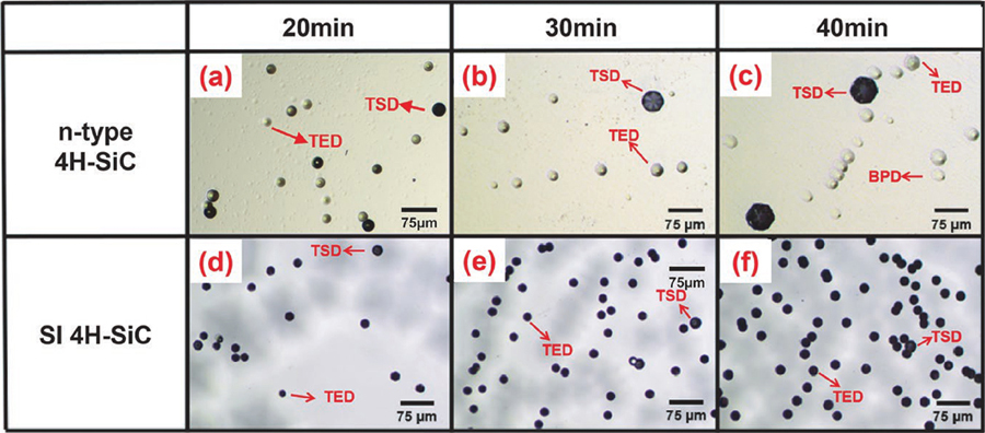
After molten-KOH etching, etch pits are formed at the surface of 4H-SiC, as a result of the preferential etching around dislocations.Figs. 1(a)–1(c) present OM images of n-type 4H-SiC wafers subjected to molten-KOH etching with the etching durations ranging from 20 to 40 min. As the etching time increases, the average size of etch pits increases. According to the traditional discrimination approach, the large hexagonal pits, small hexagonal pits and sea-shell shaped pits are attributed to the etch pits of TSDs, TEDs, and BPDs, respectively. The Burgers vectors for TSD and TED are
and
, respectively. The strain field surrounding the TSD is larger than that of the TED. Therefore, the size of etch pits of TSDs are larger than those of TEDs. Due to the 4.0° off-axis slicing of n-type 4H-SiC, the etch pits of TEDs deviate from regular hexagon or circle, and confuse with those of BPDs.Figs. 1(d)–1(f) display OM images of SI 4H-SiC wafers subjected to molten-KOH etching with the etching durations ranging from 20 to 40 min. It can be seen that the etch pits of TDs are similar. Even for SI 4H-SiC etched by molten KOH for 40 min, the average size ratio of TSDs and TEDs is only 1.1−1.2. More significantly, TMDs are not found with the approach.

Figure 1.(Color online) Representative OM images of etched 4H-SiC samples. The doping profiles and etching durations are labelled in etch figure.
We then investigate the effect of etching additives on the discrimination of dislocations in 4H-SiC, with the etching duration of 30 min. For n-type 4H-SiC samples, K2CO3 reduces the etching rate of KOH and decreases the average size of etch pits in 4H-SiC. K2CO3 also enlarges the size difference between TDs [Fig. 2 (b)]. Na2O2 are found to increase the etching rate and increase the average size of etch pits [Fig. 2(c)]. These results agree well with previous research[26,27]. Due to the high etching rate of SI 4H-SiC, the effect of additives on the etching rate of SI 4H-SiC is not that obvious compared to what happens in n-type 4H-SiC. For SI 4H-SiC, neither K2CO3 nor Na2O2 enlarges the etch-pit morphology difference among different dislocations. Therefore, additives only change the size difference for etch pits of dislocations, but exerts negligible effect on the discrimination of dislocations in 4H-SiC.
Figure 2.(Color online) Representative OM images of molten-KOH etched 4H-SiC with the etching duration of 30 min. The doping of 4H-SiC and molten additives are labelled in the figure.
From above analysis, we find that the two-dimensional morphology cannot discriminate TDs and BPDs in SI and n-type 4H-SiC. We then characterize the three-dimensional morphology of etch pits by LSCM. As shown inFig. 3, there are three kinds of etch pits in molten-KOH etched n-type 4H-SiC. Consistent with OM observations, the larger hexagonal etch pits are attributed to etch pits of TSDs. The depth for the etch pit of TSD is more than 10μm, and the slope is unitarily steep throughout the etch pit, with the value of the inclination angles (θ) being 34.05° [Fig. 3(a)]. The size of the etch pit of a TED is relatively small. Due to the off-axis slicing of n-type 4H-SiC, the etch pit of TED is oval shaped, with the major axis and minor axis being 25 and 22μm, respectively [Fig. 3 (b)]. The depth profile for the TED etch pit is a nonregular triangle, with the depth being 2.4μm, and the value of the inclination angle being 7.18° [Fig. 3(b)]. We find that the etch pits of BPDs are relatively smaller and shallower than those of TEDs. As shown inFig. 3(c), the major-axis size, minor-axis size and inclination angle for the etch pit of the BPD are 23μm, 18μm, and 2.70°, respectively.
Figure 3.(Color online) The LSCM images and depth profiles of (a) TSD, (b) TED, and (c) BPD.
With this discussion, we investigate the distribution of sizes and inclination angles of etch pits in molten-KOH etched 4H-SiC with the etching temperature of 550 °C and the etch duration of 30 min. For molten-KOH etched n-type 4H-SiC, the size distribution for the etch pits of TEDs and TSDs clearly separated, while the size distribution for the etch pits of TEDs and BPDs partially overlapped with each other [Fig. 4(a)]. This indicates that the size of etch pits cannot discriminate TEDs from BPDs in n-type 4H-SiC. We find that the values of inclination angles (θ) for the etch pits of TSDs, TEDs and BPDs are in the ranges of 27°−35°, 8°−15° and 2°−4°, respectively [Fig. 4(a)]. This indicates that the dislocations in n-type 4H-SiC are successfully discriminated by verifying the inclination angles of the etch pits of dislocations. In SI 4H-SiC, the size distribution of the etch pits of TEDs and TSDs partially overlapped with each other, while the inclination angles (θ) for the etch pits of TEDs and TSDs are in the ranges of 31°−34° and 21°−24°, respectively [Fig. 4(b)], which is similar to Katsunoet al.’s results[41]. This also indicates that dislocations in SI SiC are also well discriminated by the inclination angles of the etch pits. However, because the SI wafers used for the experiments are on-axis, the BPD data are not available.
Figure 4.(Color online) The relationship between the sizes and inclination angles of the etch pits in (a) n-type SiC and (b) SI SiC.
To verify the effectiveness of discriminating dislocations by verifying the inclination angles of etch pits, and compare the approaches to discriminate dislocations by verifying the sizes and inclination angles of etching pits, we investigate the change of the size and inclination angles of etch pits when the etching duration from 10 to 60 min. As shown inFig. 5(a), the average size of etch pits of TDs and BPDs in both n-type and SI 4H-SiC continually increases with the etching duration. This makes it difficult to establish an absolute value to discriminate TDs and BPDs by verifying the size of etch pits of dislocations. However, the inclination angles of etch pits in both n-type and SI 4H-SiC basically do not change with the etching duration [Fig. 5(b)]. Therefore, the discrimination of TSDs, TEDs, and BPDs can be realized by verifying the inclination angles of etch pits, which does not depend on the etching durations. This means that by verifying the inclination angles of etch pits, one can discriminate dislocations in 4H-SiC without optimizing the etching durations.
Figure 5.(Color online) The average (a) size and (b) inclination angle of etch pits of different dislocations as functions of the etching duration in both n-type and SI 4H-SiC.
Besides these common etch pits, we find a new kind of etch pits. As shown inFigs. 6(a) and6(b), the new etch pits have similar etch-pit size of TSDs. Unlike TSDs, the bottom of the new etch pit is a small circular plane. As shown inFigs. 6(c) and6(d), the depth profile of the new etch pit can be divided into two parts: the slope for deep center of the new etch pit is relatively gentle, with the inclination angle (θ1) being 28°. The slope of the outer fringe is steeper than that of the deep center, with the inclination angle (θ2) being 9°. According to the distribution for the inclination angles of etch pits of TSDs and TEDs, we attribute the new etch pit to the etch pit of TMD. The Burgers vector of the TMD isc +a, therefore, it can be regarded that TMD is the mixture of the TSD and TED. During the molten-KOH etching, the highly stained atoms along the spiral dislocation line are firstly removed, resulting in the larger size and the steep slope of the outer fringe for the etch pit of TMD. As the etching process continues, the atoms surrounding TEDs with lower strain begin to be removed. The etching along the TED-characterized dislocation line rise to the gentle slope and terminal point at the center of the etch pit of TMD.
Figure 6.(Color online) (a) OM, (b) AFM, and (c) LSCM images of a representative TMD. (d) Depth profile of the TMD.
To further explain that the etch pit is of the TMD etch pit. The dislocation line of etch pit was analyzed by the TBDF method through observation from different directions by inclining the sample. We find that the dislocation line is visible both atg = 0002 [Fig. 7(a)] andg =
[Fig. 7(b)]. This indicates the Burgers vector of TMD has bothc anda components, which verifies the mixing Burger vector of the TMD.
Figure 7.(Color online) TEM images at (a)g = 0004 and (b)g =
of the etch pit of TMD.
Conclusion
We have investigated the effect of etching durations and etching additives on the morphologies of molten-KOH etched pits of different dislocations in 4H-SiC. We find that the inclination angles of dislocation-related etch pits are independent of the etching duration, which facilitates the discrimination of different dislocations and statistic of dislocation densities in 4H-SiC. Therefore, the inclination angles of the etch pits of molten-alkali etched 4H-SiC can be adopted to discriminate TSDs, TEDs and BPDs in 4H-SiC. In n-type 4H-SiC, the inclination angles for the etch pits of TSDs, TEDs, and BPDs in molten-alkali etched 4H-SiC are in the range of 27°−35°, 8°−15° and 2°−4°, respectively. In SI 4H-SiC, the inclination angles for the etch pits of TSDs and TEDs are in the range of 31°−34° and 21°−24°, respectively. More significantly, the inclination angles of TMD are found to consist of TED-characterized angle and TSD-characterized angle. Within this approach, TMDs are distinguished from TSDs, which paves the way for further investigations on the role of TMDs in the performances of 4H-SiC.
References
[1] J B Casady, R W Johnson. Status of silicon carbide (SiC) as a wide-bandgap semiconductor for high-temperature applications: A review. Solid State Electron, 39, 1409(1996).
[2] N G Wright, A B Horsfall, K Vassilevski. Prospects for SiC electronics and sensors. Mater Today, 11, 16(2008).
[3] J Yoon, K Kim. A 3.3 kV 4H-SiC split gate MOSFET with a central implant region for superior trade-off between static and switching performance. J Semicond, 42, 062803(2021).
[4] I G Yeo, W S Yang, J H Park et al. Two-inch a-plane (11-20) 6H-SiC crystal grown by using the PVT method from a small rectangular substrate. J Korean Phy Soc, 58, 1541(2011).
[5] X She, A Q Huang, Ó Lucía et al. Review of silicon carbide power devices and their applications. IEEE Trans Ind Electron, 64, 8193(2017).
[6] X Wang, Y W Zhong, H B Pu et al. Investigation of lateral spreading current in the 4H-SiC Schottky barrier diode chip. J Semicond, 42, 112802(2021).
[7] D M Lukin, C Dory, M A Guidry et al. 4H-silicon-carbide-on-insulator for integrated quantum and nonlinear photonics. Nat Photonics, 14, 330(2020).
[8] Bardeleben H J von, J L Cantin, A Csóré et al. NV centers in 3C, 4H, and 6H silicon carbide: A variable platform for solid-state qubits and nanosensors. Phys Rev B, 94, 121202(2016).
[9] H B Banks, Ö O Soykal, R L Myers-Ward et al. Resonant optical spin initialization and readout of single silicon vacancies in 4H-SiC. Phys Rev Appl, 11, 024013(2019).
[10] J F Wang, F F Yan, Q Li et al. Coherent control of nitrogen-vacancy center spins in silicon carbide at room temperature. Phys Rev Lett, 124, 223601(2020).
[11] J F Wang, F F Yan, Q Li et al. Robust coherent control of solid-state spin qubits using anti-Stokes excitation. Nat Commun, 12, 3223(2021).
[12] S Ha, M Benamara, M Skowronski et al. Core structure and properties of partial dislocations in silicon carbide p-i-n diodes. Appl Phys Lett, 83, 4957(2003).
[13] M Abadier, R L Myers-Ward, N A Mahadik et al. Nucleation of in-grown stacking faults and dislocation half-loops in 4H-SiC epitaxy. J Appl Phys, 114, 123502(2013).
[14] Q Wahab, A Ellison, A Henry et al. Influence of epitaxial growth and substrate-induced defects on the breakdown of 4H-SiC Schottky diodes. Appl Phys Lett, 76, 2725(2000).
[15] P G Neudeck, J A Powell. Performance limiting micropipe defects in silicon carbide wafers. IEEE Electron Device Lett, 15, 63(1994).
[16] A Grekov, Q C Zhang, H Fatima et al. Effect of crystallographic defects on the reverse performance of 4H-SiC JBS diodes. Microelectron Reliab, 48, 1664(2008).
[17] P G Neudeck, W Huang, M Dudley. Study of bulk and elementary screw dislocation assisted reverse breakdown in low-voltage (<250 V) 4H-SiC p+n junction diodes. I. DC properties. IEEE Trans Electron Devices, 46, 478(1999).
[18] R E Stahlbush, M E Twigg, J J Sumakeris et al. Mechanisms of stacking fault growth in SiC PiN diodes. MRS Online Proc Libr, 815, 241(2004).
[19] S Ha, H J Chung, N T Nuhfer et al. Dislocation nucleation in 4H silicon carbide epitaxy. J Cryst Growth, 262, 130(2004).
[20] D Zhuang, J H Edgar. Wet etching of GaN, AlN, and SiC: a review. Mater Sci Eng R, 48, 1(2005).
[21] K Christiansen, R Helbig. Anisotropic oxidation of 6H-SiC. J Appl Phys, 79, 3276(1996).
[22] W Geng, G Yang, X Zhang et al. Identification of subsurface damages of 4H-SiC wafers by combining photo-chemical etching and molten-alkali etching. J Semicond, 43, 102801(2022).
[23] R W Brander, A L Boughey. The etching of-silicon carbide. Br J Appl Phys, 18, 905(1967).
[24] L Dong, L Zheng, X F Liu et al. Defect revelation and evaluation of 4H silicon carbide by optimized molten KOH etching method. Mater Sci Forum, 740, 243(2013).
[25] J J Li, H Luo, G Yang et al. Nitrogen decoration of basal-plane dislocations in 4H-SiC. Phys Rev Appl, 17, 054011(2022).
[26] M Katsuno, N Ohtani, J Takahashi et al. Mechanism of molten KOH etching of SiC single crystals: Comparative study with thermal oxidation. Jpn J Appl Phys, 38, 4661(1999).
[27] S A Sakwe, R Müller, P J Wellmann. Optimization of KOH etching parameters for quantitative defect recognition in n- and p-type doped SiC. J Cryst Growth, 289, 520(2006).
[28] Y Z Yao, Y Ishikawa, Y Sugawara et al. Molten KOH etching with Na 2O 2additive for dislocation revelation in 4H-SiC epilayers and substrates. Jpn J Appl Phys, 50, 075502(2011).
[29] D Siche, D Klimm, T Hölzel et al. Reproducible defect etching of SiC single crystals. J Cryst Growth, 270, 1(2004).
[30] Y Yang, Z Z Chen. Defect characterization of SiC by wet etching process. J Synth Cryst, 37, 634(2008).
[31] H Z Song, T S Sudarshan. Basal plane dislocation mitigation in SiC epitaxial growth by nondestructive substrate treatment. Cryst Growth Des, 12, 1703(2012).
[32] H Luo, J J Li, G Yang et al. Electronic and optical properties of threading dislocations in n-type 4H-SiC. ACS Appl Electron Mater, 4, 1678(2022).
[33] J Takahashi, M Kanaya, Y Fujiwara. Sublimation growth of SiC single crystalline ingots on faces perpendicular to the (0001) basal plane. J Cryst Growth, 135, 61(1994).
[34] Y Gao, Z H Zhang, R Bondokov et al. The effect of doping concentration and conductivity type on preferential etching of 4H-SiC by molten KOH. MRS Online Proc Libr, 815, 6(2004).
[35] Y Zhang, H Chen, D Z Liu et al. High efficient polishing of sliced 4H-SiC (0001) by molten KOH etching. Appl Surf Sci, 525, 146532(2020).
[36] Y X Cui, X B Hu, X J Xie et al. Threading dislocation classification for 4H-SiC substrates using the KOH etching method. CrystEngComm, 20, 978(2018).
[37] D Nakamura, S Yamaguchi, I Gunjishima et al. Topographic study of dislocation structure in hexagonal SiC single crystals with low dislocation density. J Cryst Growth, 304, 57(2007).
[38] K Konishi, Y Nakamura, A Nagae et al. Direct observation and three dimensional structural analysis for threading mixed dislocation inducing current leakage in 4H-SiC IGBT. Jpn J Appl Phys, 59, 011001(2020).
[39] Y Z Yao, Y Ishikawa, Y Sugawara et al. Correlation between etch pits formed by molten KOH+Na 2O 2 etching and dislocation types in heavily doped n +-4H-SiC studied by X-ray topography. J Cryst Growth, 364, 7(2013).
[40] K Fukunaga, S D Jun, T Kimoto. Anisotropic etching of single crystalline SiC using molten KOH for SiC bulk micromachining. Micromachining and Microfabrication Process Technology XI(2006).
[41] T Katsuno, Y Watanabe, F Hirokazu et al. New separation method of threading dislocations in 4H-SiC epitaxial layer by molten KOH etching. Mater Sci Forum, 679/680, 298(2011).