Abstract
Planar ring resonator waveguides are fabricated in thin films of chalcogenide glass, deposited on silica-on-silicon substrates. Waveguide cores are directly written by scanning the focused illumination of a femtosecond Ti:sapphire laser at a central wavelength of 810 nm, through a two-photon photo-darkening process. A large photo-induced index change of 0.3–0.4 refractive index units is obtained. The radius of the ring resonator is 1.9 mm, corresponding to a transmission free spectral range of 9.1 GHz. A high loaded (intrinsic) value of 110,000 (180,000) is achieved. The thermal dependence of the resonator transfer function is characterized. The results provide the first report, to the best of our knowledge, of directly written high- ring resonators in chalcogenide glass films, and demonstrate the potential of this simple technique towards the fabrication of planar lightguide circuits in these materials.1. INTRODUCTION
Chalcogenides are a category of glass compounds that contain one of the chalcogen elements: S, Se, or Te. Chalcogenides are drawing increased attention in research and applications, due to their remarkable electrical and optical properties. Although amorphous, they can be semiconducting and display bandgap behavior [1,2]; they are characterized by a broad transparency window, from the visible to the middle infrared [3]; their refractive index can be as high as 3.5 refractive index units (RIU) [4]; and their nonlinear refractive index, Raman scattering, and Brillouin scattering coefficients are 100–1000 times larger than the corresponding values in silica [4–6]. Lastly, chalcogenide glasses are highly photosensitive [7,8]: direct laser-beam illumination of these glasses could cause permanent material changes, ranging from refractive index variations [9,10] through to reflow and mass transfer [11–14], depending on wavelength and intensity. Chalcogenides therefore constitute a favorable material platform for all-optical signal processing and sensing applications [15–18].
Fabrication technologies of planar lightguide circuits (PLCs) in chalcogenide glasses include lithography and dry etching [19], lift-off processes [20], thermal nano-imprinting [21,22], and direct laser-beam writing [23–28]. Direct laser-beam writing relies on the photo-darkening effect in chalcogenides to introduce a local increase in the refractive index of core regions. The process is simple, does not involve the exposure of the glass materials to chemicals, and does not introduce sidewall roughness. On the other hand, linear losses of directly written waveguides in chalcogenide glasses are higher than those of etched devices [19], and comparatively small index contrasts might lead to additional bending losses.
Ring resonator structures in PLCs of various electro-optic materials are widely employed as the basis for narrowband filters [29], recirculating delay lines [30], electro-optic modulators [31], and laser cavities [32]. The high sensitivity of the ring cavity to the refractive index of its surroundings is used in biochemical sensors [33]. Cavity enhancement of the pronounced nonlinearities of chalcogenides holds much promise in all-optical signal processing. Ring resonators were fabricated in chalcogenides using a lift-off process, with a reported of 10,000 [20]. Recently, loaded (unloaded) values of 150,000 (390,000) were achieved in As–Se family glass resonators of 100 μm radius using a nano-imprint fabrication method [21], and unloaded of 460,000 was obtained in micro-disc resonators [22]. racetrack resonators were also fabricated on top of underlying waveguides [34]. The fabrication of high- ring resonators in chalcogenides using direct laser-beam lithography has not yet been reported.
Sign up for Photonics Research TOC. Get the latest issue of Photonics Research delivered right to you!Sign up now
Herein we present the fabrication and characterization of ring resonators in thin films. Waveguide cores are defined using femtosecond Ti:sapphire laser illumination [10,26]. A large index modification of 0.4 RIU is achieved. The radius of the ring resonators is approximately 1.9 mm, providing a free spectral range (FSR) of 9.1 GHz. The transfer function of the ring resonators corresponds to a loaded (unloaded) value of 110,000 (180,000). The results demonstrate the applicability of direct laser-beam lithography to the fabrication of chalcogenide glass PLCs for all-optical signal processing and sensing applications.
2. CHARACTERIZATION OF PHOTO-INDUCED INDEX CHANGES
The layer structure of samples used in this work is shown schematically in Fig. 1. A core layer of thickness was deposited on a silica-on-silicon substrate, by thermal evaporation of a bulk target from a quartz crucible in a Torr vacuum [35,36]. The thicknesses of the underlying silica layer and of the silicon substrate were and , respectively. The refractive indices of , silica, and silicon at 1550 nm wavelength are RIU, RIU, and RIU respectively.
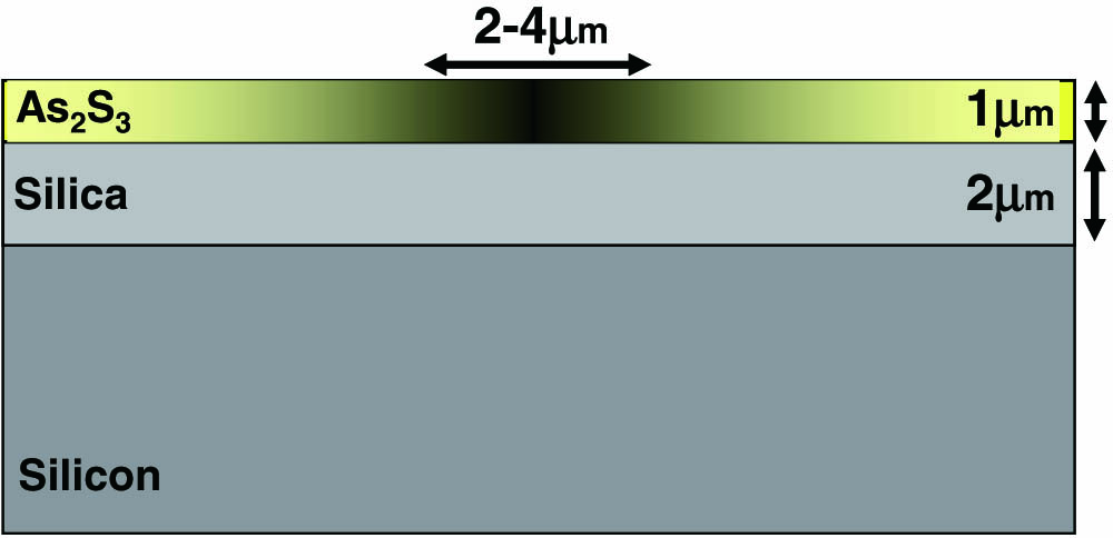
Figure 1.Schematic illustration of the layer structure of samples used in this work and an illustration of the transverse profile of photo-induced refractive index changes in the core glass layer.
Waveguide cores were directly written in the chalcogenide film by femtosecond Ti:sapphire laser illumination, operating at a central wavelength of 810 nm. The sub-bandgap irradiation introduces a permanent increase in the local refractive index through a two-photon, photo-darkening process [10,26]. The writing laser pulses were 200 fs long, and their repetition rate was 80 MHz. The laser beam was focused through a microscope objective lens (numerical aperture of 0.7). The average power of the focused beam was attenuated to 5 mW, and its intensity was . During illumination, the -coated sample was translated through the focal point of the beam by a computer-controlled, three-axis piezo-electric stage, at 4 μm/s speed.
The definition of ring resonators with radius required the controlled translation of the sample with submicrometer accuracy over several hours. To that end, a closed-loop positioning system was constructed. A fixed camera tracked the exact location of the illumination spot of an external light-emitting diode on the surface of the three-axis stage, and corrected the positioning of the stage motors for possible drifting. In addition, the translation stages were designed for thermal compensation.
The local increase in the refractive index of illuminated regions was estimated using auxiliary transmission measurements, illustrated in Fig. 2. An -coated silica-on-silicon sample was held perpendicular between two collimated fibers. The refractive index within a pattern in the chalcogenide layer of the sample under test was modified through the direct writing of 150 adjacent linescans, using the above illumination parameters. Light from the output port of an optical vector network analyzer (OVA) at 1550 nm wavelength range was launched towards the bottom surface of the silicon substrate through one fiber, at normal incidence. Light transmitted through the top surface of the sample was collected by the second fiber, and analyzed by the OVA. The measurement configuration represents a modification of the Swanepoel method for the determination of the refractive index of thin films [37].

Figure 2.Schematic illustration of the setup used in measurements of the photo-induced refractive index change in films.
Figure 3 (top) shows the measured transmission through the sample under test as a function of wavelength, both within and outside the irradiated pattern. The transmission through the sample is dominated by reflections at the top and bottom surfaces, which introduce a response of a low-finesse Fabry–Perot etalon. The FSR of the transmission spectrum in reference regions that were not illuminated can be approximated as , where is the central wavelength and denotes the optical path length through the sample. The measured is 0.86 nm. The FSR of transmission through the photo-darkened region is modified by
Figure 3.Top: OVA measurements of the transmission of light through the layers of a silica-on-silicon sample coated with an film (see Fig. 2). The red (blue) curve corresponds to a region outside (within) a photo-darkened area. Bottom: spectral offset in nanometers between peaks of maximum transmission outside and within the photo-darkened area. The linearly increasing offset corresponds to an increase in the refractive index within the photo-darkened region by 0.4 RIU.
Let us denote the wavelengths of maximum transmission as , where is an integer. Figure 3 (bottom) shows the offsets between the transmission spectra of reference and illuminated regions, for 50 FSR periods in the range of 1530–1570 nm. The slope of the curve represents of 0.338 pm. Direct writing therefore increases the refractive index of the layer by RIU, to approximately 2.8 RIU. The observed photo-induced is five times larger than that observed in [10]. Note, however, that the accumulated laser irradiation in [] used in this work is orders of magnitude larger. Photo-darkening-induced index changes of comparable magnitude in chalcogenides are known in the literature [36,38,39]. Bending losses in rings of millimeter-scale radii and such large values are negligible.
The modal profiles of directly written waveguides at different wavelengths were calculated using COMSOL multiphysics simulations. The waveguide supports multiple transverse-electric (TE) and transverse-magnetic (TM) modes; however, the coupling of light from tapered fibers to higher-order modes is considerably weaker [26] than coupling into the fundamental modes. Figure 4 shows the calculated effective indices and group indices of the fundamental TE and TM modes of a 4-μm-wide waveguide at 1550 nm wavelength, as a function of the photo-induced core . The expected values of the group indices of the fundamental TM and TE modes, with set to 0.4 RIU, are 2.9 and 2.85 RIU, respectively. For the relatively broad core widths of 2–4 μm, and for the comparatively large , the exact profile of graded-index variations has a negligible effect on the calculated indices.
Figure 4.Calculated effective indices (red) and group indices (blue) of the fundamental modes of directly written waveguides in thin films, as a function of the photo-induced refractive index change in the core region . Solid (dashed) lines correspond to the TM (TE) mode.
A top-view microscope image of segments of ring and bus waveguides is shown in Fig. 5. The width of the straight bus waveguide core is on the order of 2 μm, whereas that of the ring is approximately 4 μm. The broader width of the ring waveguide is due to its lower scanning speed using alternating and translation steps. The separation between the centers of bus and ring waveguides is approximately 2 μm, optimized for maximum extinction ratio (ER) in the transmission frequency response of the devices (see below). Figure 6 shows a top-view image of a ring resonator device of 200 μm radius, with red light coupled in for illustration purposes only. The radius of the specific ring used in subsequent characterization was measured as 1.888 mm, by precise translation of the sample under a microscope with large magnification.
Figure 5.Top-view microscope image of parts of bus and ring waveguides, directly written in a thin layer of .
Figure 6.Top view of a ring resonator waveguide, directly written in an thin film. Red light is coupled from a tapered fiber for illustration purposes only.
3. TRANSFER FUNCTION MEASUREMENTS
The spectral transfer function of the ring resonator was measured using the OVA, with a spectral resolution of 2 pm. Light was coupled in and out of the devices using tapered fibers with a modal radius of 2 μm. The coupling losses to/from the devices at 1550 nm varied between 3 and 5 dB per facet, depending on the facet’s quality. Figure 7 shows the OVA measurement of the infinite impulse response of the ring resonator in the time domain. The 110 ps delay between successive impulses corresponds to a group index of 2.8 RIU, in general agreement with simulations. The measured group delay corresponds to a photo-induced value of 0.3–0.35 RIU (see Fig. 4). The attenuation between successive impulses is given by , where is the coupling coefficient between the bus and ring waveguides, denotes the loss coefficient per unit length, and is the circumference of the ring. The measurements suggest that .
Figure 7.OVA measurement of the temporal impulse response of a ring resonator of 1.888 mm radius, directly written in a thin film of .
Figure 8 (top) shows the measured spectral power transfer function of the ring resonator. A FSR of 9.1 GHz is observed, with an ER that reaches 25 (14 dB). Figure 8 (bottom) shows a magnified view of one spectral transmission notch. The full width at half maximum (FWHM) of the transmission notches is 14 pm, which corresponds to a loaded value of approximately 110,000. The unloaded value and the loss coefficient may be estimated using the following relations [40]: where and denote the loaded and unloaded values, respectively. The relatively high value of is an order of magnitude better than that reported using a lift-off fabrication process [20], and a factor of 2 lower than the values obtained recently in As–Se glasses using thermal nano-imprinting [21,22].
Figure 8.Top: OVA measurement of the spectral power transfer function of a ring resonator of 1.888 mm radius, directly written in a thin film of . Bottom: magnified view of a single transmission notch, with a FWHM of 0.014 nm.
Figure 9 shows the spectral power transfer functions of the ring resonator at different temperatures of an actively controlled mount. The observed thermal offset of a given resonance wavelength was . The thermal offset is given by where is the thermo-optic coefficient of and denotes the coefficient of linear thermal expansion. Values of [41] and [42] appear in the literature. Based on these values, a larger thermal change of 0.060 nm/°C in the resonance wavelength could be expected. The reasons for this difference require further investigation. A possible explanation could be due to thermal expansion of the entire layer structure, which might be different from that of bulk .
Figure 9.OVA measurements of the spectral power transfer function of a ring resonator of 1.888 mm radius, at several temperatures (in °C, see legend). The resonance wavelengths are offset by 0.022 nm/°C.
The transfer function of the device was monitored over more than one year of storage in a standard laboratory environment. No changes were noted in or . The devices support a coupled average power of 200 mW, and 500-ns-long pulses with coupled peak power of 2 W, without damage.
4. CONCLUSION
In summary, this work provides the first report, to the best of our knowledge, of high- ring resonators in glass PLCs, fabricated using direct laser-beam writing. The simple fabrication of high-quality resonators in highly nonlinear media carries much promise for all-optical signal processing applications. Ongoing work is being dedicated to the fabrication of resonators having different values of , and to attempts to reduce losses. Losses may be improved with the deposition of upper capping layers, such as silica, which might prevent oxidization of the chalcogenide glass surface. Lastly, nonlinear propagation effects in the resonator devices are being investigated.
References
[1] B. T. Kolomiets. Vitreous semiconductors I. Phys. Status Solidi, 7, 359-372(1964).
[2] B. T. Kolomiets. Vitreous semiconductors II. Phys. Status Solidi, 7, 713-731(1964).
[3] R. Frerichs. New optical glasses with good transmission in the infrared. J. Opt. Soc. Am., 43, 1153-1157(1953).
[4] K. Ogusu, J. Yamasaki, S. Maeda, M. Kitao, M. Minakata. Linear and nonlinear optical properties of Ag-As-Se chalcogenide glasses for all-optical switching. Opt. Lett., 29, 265-267(2004).
[5] J. S. Sanghera, I. D. Aggarwal, L. B. Shaw, C. M. Florea, P. Pureza, V. Q. Nguyen, F. Kung, I. D. Aggarwal. Nonlinear properties of chalcogenide glass fibers. J. Optoelectron. Adv. Mater., 8, 2148-2155(2006).
[6] A. Zakery, S. R. Elliot. Optical properties and applications of chalcogenide glasses: a review. J. Non-Cryst. Solids, 330, 1-12(2003).
[7] E. Owen, A. P. Firth, P. J. S. Ewen. Photo-induced structural and physico-chemical changes in amorphous chalcogenide semiconductors. Philos. Mag. B, 52, 347-362(2006).
[8] J. D. Musgraves, K. Richardson, H. Jain. Laser-induced structural modification, its mechanisms, and applications in glassy optical materials. Opt. Mater. Express, 1, 921-935(2011).
[9] V. I. Mikla. Photoinduced structural changes and related phenomena in amorphous arsenic chalcogenides. J. Phys. Condens. Matter, 8, 429-448(1996).
[10] A. Zoubir, M. Richardson, C. Rivero, A. Schulte, C. Lopez, K. Richardson. Direct femtosecond laser writing of waveguides in As2S3 thin films. Opt. Lett., 29, 748-750(2004).
[11] Y. Kaganovskii, D. L. Beke, S. Charnovych, S. Kokenyesi, M. L. Trunov. Inversion of the direction of photo-induced mass transport in As20Se80 films: experiment and theory. J. Appl. Phys., 110, 063502(2011).
[12] A. Saliminia, T. V. Galstian, A. Villeneuve. Optical field-induced mass transport in As2S3 chalcogenide glasses. Phys. Rev. Lett., 85, 4112-4115(2000).
[13] M. L. Trunov, P. M. Lytvyn, P. M. Nagy, O. M. Dyachyns’ka. Real-time atomic force microscopy imaging of photoinduced surface deformation in AsSe chalcogenide films. Appl. Phys. Lett., 96, 111908(2010).
[14] M. L. Trunov, P. M. Lytvyn, O. M. Dyachyns’ka. Alternating matter motion in photoinduced mass transport driven and enhanced by light polarization in amorphous chalcogenide films. Appl. Phys. Lett., 97, 031905(2010).
[15] B. J. Eggleton, B. Luther-Davies, K. Richardson. Chalcogenide photonics. Nat. Photonics, 5, 141-148(2011).
[16] V. Ta’eed, N. J. Baker, L. Fu, K. Finsterbusch, M. R. E. Lamont, D. J. Moss, H. C. Nguyen, B. J. Eggleton, D.-Y. Choi, S. Madden, B. Luther-Davies. Ultrafast all-optical chalcogenide glass photonic circuits. Opt. Express, 15, 9205-9221(2007).
[17] M. D. Pelusi, F. Luan, S. Madden, D.-Y. Choi, D. A. Bulla, B. Luther-Davies, B. J. Eggleton. Wavelength conversion of high-speed phase and intensity modulated signals using a highly nonlinear chalcogenide glass chip. IEEE Photon. Technol. Lett., 22, 3-5(2010).
[18] M. Galili, J. Xu, H. C. H. Mulvad, L. K. Oxenløwe, A. T. Clausen, P. Jeppesen, B. L. Davies, S. Madden, A. Rode, D. Y. Choi, M. Pelusi, F. Luan, B. J. Eggleton. Breakthrough switching speed with an all-optical chalcogenide glass chip: 640 Gbit/s demultiplexing. Opt. Express, 17, 2182-2187(2009).
[19] S. J. Madden, D.-Y. Choi, D. A. Bulla, A. V. Rode, B. Luther-Davies, V. G. Ta’eed, M. D. Pelusi, B. J. Eggleton. Long, low loss etched As2S3 chalcogenide waveguides for all-optical signal regeneration. Opt. Express, 15, 14414-14421(2007).
[20] J. Hu, N. Carlie, L. Petit, A. Agarwal, K. Richardson, L. Kimerling. Demonstration of chalcogenide glass racetrack microresonator. Opt. Lett., 33, 761-763(2008).
[21] Y. Zou, D. Zhang, H. Lin, L. Li, L. Moreel, J. Zhou, Q. Du, O. Ogbuu, S. Danto, J. D. Musgraves, K. Richardson, K. D. Dobson, R. Birkmire, J. Hu. High-performance, high-index-contrast chalcogenide glass photonics on silicon and unconventional non-planar substrate. Adv. Opt. Mater., 2, 478-486(2014).
[22] L. Li, H. Lin, S. Qiao, Y. Zou, S. Danto, K. Richardson, J. D. Musgraves, N. Lu, J. Hu. Integrated flexible chalcogenide glass photonic devices. Nat. Photonics, 8, 643-649(2014).
[23] T. Li, K. Turcotte, J. M. Laniel, A. Villeneuve, C. Lopez, K. Richardson. Fabrication and characterization of chalcogenide optical waveguides. Integrated Photonics Research, 45, IFH4(2000).
[24] O. M. Efimov, L. B. Glebov, K. A. Richardson, E. Van Stryland, T. Cardinal, S. H. Park, M. Couzi, J. L. Bruneel. Waveguide writing in chalcogenide glasses by a train of femtosecond laser pulses. Opt. Mater. (Amsterdam), 17, 379-386(2001).
[25] X. Gai, T. Han, A. Prasad, S. Madden, D.-Y. Choi, R. Wang, D. Bulla, B. Luther-Davies. Progress in optical waveguides fabricated from chalcogenide glasses. Opt. Express, 18, 26635-26646(2010).
[26] S. Levy, V. Lyubin, M. Klebanov, J. Scheuer, A. Zadok. Stimulated Brillouin scattering amplification in centimeter-long directly written chalcogenide waveguides. Opt. Lett., 37, 5112-5114(2012).
[27] A. Saliminia, A. Villeneuve, T. V. Galstyan, S. LaRochelle, K. Richardson. First-and second-order Bragg gratings in single-mode planar waveguides of chalcogenide glasses. J. Lightwave Technol., 17, 837-842(1999).
[28] N. Hô, M. C. Phillips, H. Qiao, P. J. Allen, K. Krishnaswami, B. J. Riley, T. L. Myers, N. C. Anheier. Single-mode low-loss chalcogenide glass waveguides for the mid-infrared. Opt. Lett., 31, 1860-1862(2006).
[29] Q. Li, M. Soltani, S. Yegnanarayanan, A. Adibi. Design and demonstration of compact, wide bandwidth coupled-resonator filters on a siliconon- insulator platform. Opt. Express, 17, 2247-2254(2009).
[30] H. Park, J. P. Mack, D. J. Bluementhal, J. E. Bowers. An integrated recirculating optical buffer. Opt. Express, 16, 11124-11131(2008).
[31] Q. Xu, B. Schmidt, S. Pradhan, M. Lipson. Micrometre scale silicon electro-optic modulator. Nature, 435, 325-327(2005).
[32] W. Fang, R. Jones, H. Park, O. Cohen, O. Raday, M. J. Paniccia, J. E. Bowers. Integrated AlGaInAs-silicon evanescent racetrack laser and photodetector. Opt. Express, 15, 2315-2322(2007).
[33] M. Armani, R. P. Kulkarni, S. E. Fraser, R. C. Flagan, K. J. Vahala. Label-free single-molecule detection with optical microcavities. Science, 317, 783-787(2007).
[34] M. E. Solmaz, D. B. Adams, W. C. Tan, W. T. Snider, C. K. Madsen. Vertically integrated As2S3 ring resonator on LiNbO3. Opt. Lett., 34, 1735-1737(2009).
[35] I. Abdullhalim, M. Gelbaor, M. Klebanov, V. Lyubin. Photoinduced phenomena in nano-dimentional glassy As2S3 films. Opt. Mater. Express, 1, 1192-1201(2011).
[36] B. Spektor, J. Shamir, V. Lyubin, M. Klebanov. Recording on As2S3 glassy films by pulsed and continuous illumination—optical evaluation and comparison. Opt. Eng., 42, 3279-3284(2003).
[37] R. Swanepoel. Determination of the thickness and optical constants of amorphous silicon. J. Phys. E, 16, 1214-1222(1983).
[38] G. Pfeiffer, M. A. Paesler, S. C. Agrawal. Reversible photodarkening of amorphous arsenic chalcogens. J. Non-Cryst. Solids, 130, 111-143(1991).
[39] M. A. Iovu, M. S. Iovu, D. V. Harea, E. P. Colomeico, V. G. Ciorba. Light induced phenomena in amorphous As100-xSex and As40Se60:Sn thin films. Proc. SPIE, 6635, 663509(2007).
[40] L. W. Luo, G. S. Wiederhecker, J. Cardenas, C. Poitras, M. Lipson. High quality factor etchless silicon photonic ring resonators. Opt. Express, 19, 6284-6289(2011).
[41] A. Saliminia, T. Galstian, A. Villeneuve, K. Le Foulgoc, K. Richardson. Temperature dependence of Bragg reflectors in chalcogenide As2S3 glass slab waveguides. J. Opt. Soc. Am. B, 17, 1343-1348(2000).
[42] G. Tao. Multimaterial fibers in photonics and nanotechnology(2014).


