Motivated by the success of graphene research, atomically-thin transition metal dichalcogenide (TMDC) semiconductors are considered as promising field-effect transistor (FET) channel materials for fundamental research and potential applications. Bridging atomically-thin TMDC channels to external circuitry using metallic leads is one of the most critical steps towards high-performance devices and cutting-edge materials physics research. However, electrically interfacing semiconductor TMDC edges to metal electrodes is inherently problematic because Fermi-level pinning effects[1] naturally arise from the edge dangling bonds in metal–semiconductor junctions (Fig. 1), which deteriorate the interfacial band alignments and form high and wide Schottky barriers (Fig. 1(b)). Consequently, high contact resistance, in particular at cryogenic temperatures, seriously limits the efficiency of carrier injection into the TMDC channel and caps the available field-effect carrier mobility, making intrinsic quantum transport phenomena in this material inaccessible.

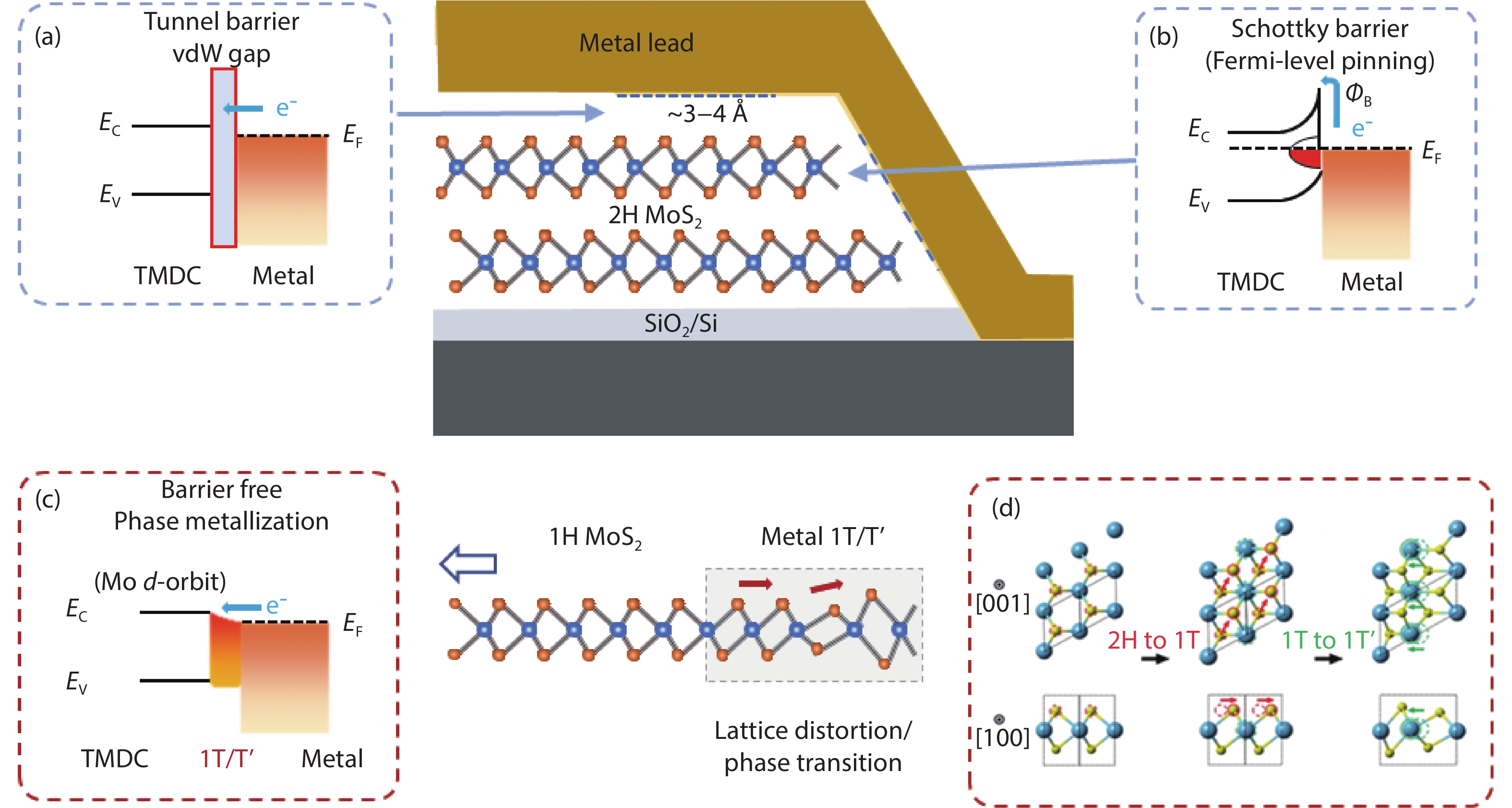
Figure 1.(Color online) Electrical interface between 2H TMDC and metal lead. (a) Interface band alignment of the van der Waals contact. (b) Interface band alignment of the Schottky-limited contact due to the presence of dangling bonds at the TMDC edge. (c) Interface band alignment of the contact based on the 1T–2H interface through locally induced phase transition. (d) Phase transition from 2H to 1T and 1T’.
In the past decade, great efforts have been made to improve the electrical contact properties of TMDC FETs by various approaches, such as direct metallization, work function matching, phase engineering, tunnel barrier structuring and van der Waals (vdW)-interfaced electrodes using mechanically-transferred metals or graphene[2, 3]. The main purpose of these efforts is to avoid the Fermi-level pinning effects. Without involving dangling bonds, the vdW junction method using metal/graphene plus extra gating on the contact region relieve the Fermi-level pinning effects and validate the Schottky-Mott limit in TMDCs[3]. However, the inherent nature of vdW contacts still limits the charge carrier injection because the interface space between the TMDC surface and the metal/graphene lead is about 3–4 Å, resulting in a tunneling barrier for current injection into the TMDC channel (Fig. 1(a)).
As shown in Figs. 2(a) and 2(b), an efficient carrier injection to the conduction bands of monolayer MoS2 requires effective orbital overlap and hybridization between Mo atoms and the metallic electrode atoms. The reason is straightforward since according to the band structure of monolayer MoS2 (Fig. 2(a)), the conduction band minimum is mainly from the contribution of the
-orbital of Mo atoms, which are sandwiched by two layers of S atoms. The
-orbital states are fully occupied, resulting in semiconductor characteristics with an energy gap. Carrier injection simply through the S surface is less efficient mainly because of two problems: (1) the barrier due to the vdW gap; and (2) the orbitals of S atoms contribute little to the conductance band edge. Therefore, injection of charge carriers through Mo atoms via orbital hybridization is the most efficient way to increase the carrier injection efficiency and elevate the performance of MoS2 FETs. To implement this scheme, partially converting the edges of semiconducting 2H-TMDCs into metallic polymorphs (e.g., 1T) has been proposed[4], which is considered as a solution to create an ideal semiconductor–metal interfaces for TMDCs since the interface between 2H and 1T can be structurally seamless without any dangling bands. The minimum energy states for 1T metallic phase are from dxz, dyz and dxy (Fig. 2(b)) which are partially occupied, resulting metallic states.
Figure 2.(Color online) (a) Band structure of monolayer MoS2. (b) The crystal structures and corresponding energy splitting diagrams of Mo/W d-orbital states before and after the phase transition. (c) The contact resistance (measured under different gate voltages Vbg) of the 3L-MoS2 FET made by oxygen-plasma-induced phase transition.
Experimentally, 1T–2H phase interfaces have been realized by phase transition using a wet chemistry doping method in MoS2[5]. However, transport measurements indicated that Schottky barrier problems still existed in the interfaces. There are a number of problems need to be further addressed. For example, the work functions between 1T and 2H bulk phases do not match each other, causing an additional barrier, and charge trapping at the 1T–2H interface exists. All these factors limit the FET device performance. Transport measurement also confirmed the contact barrier since the electrical contact performance was independent of the work functions of metal leads used to connect to the 1T phase[5]. At room temperature, the thermal-assisted carrier injection helps to overcome the 1T–2H interface barrier. However, at cryogenic temperatures, since there is no thermal-assisted carrier injection, the carrier injection efficiency is seriously limited by the Schottky barrier at the interface. Therefore, the main challenge posed to materials scientists is how to achieve a work function matched 1T–2H interface.
A number of strategies have been proposed and implemented to tackle the TMDC metallization issue, among which the soft oxygen plasma method reported by Xu et al.[6] has been verified to be an effective way to create low-temperature ohmic contacts to most popular TMDCs (MoS2, WS2, MoSe2, WSe2 and MoTe2), and interesting layer-number-dependent quantum transport phenomena[7] and large spin susceptibility[8, 9] have been discovered. The mechanism for creating low-temperature ohmic contacts by the soft oxygen plasma method is unclear since there is no interface structure information published yet. Soft oxygen plasma has been widely applied as a nondestructive way to clean some solid crystal surfaces without etching or damaging their surface structures. For boron-nitride (BN) sandwiched TMDC devices, the soft oxygen plasma selectively etches the BN layer and almost does not react with TMDCs if the plasma energy is below certain levels. Recent atomic resolution electron microscopy study carried out by Cai et al.[10] verified that fine-tuned (mainly by minimizing the plasma energy) soft oxygen plasma did not etch TMDC surfaces (similar to the analysis in Ref. [6]), but triggered lattice distortion and phase transition locally at TMDC edges/surfaces. As schematically shown in Fig. 1, the lattice distortion and phase transition involve several metallic polymorphs (1T, 1T’ or 1Td) which are formed by slightly sliding chalcogen atoms along the <110> direction and metal atoms along the <120> direction. The phase transition mechanism is complicated, possibility due to the partial replacement of chalcogen atoms by oxygen since this replacement changes local bond lengths (TM–O bonds are shorter than TM–S or TM–Se bonds; TM denotes transition metals), and thus trigger bond rearrangements or phase transitions to the metallic polymorphs without creating any lattice defects. Theoretically, TM–O bonding of 2H TMO 2 phases, such as MoO2 and WO2 have been predicted, and the replacement of chalcogen atoms by oxygen will not introduce doping effects because oxygen belongs to the chalcogen group. Moreover, the newly formed metallic polymorphs have different work functions (dimension- or size-dependent), providing a tunable parameter to modulate the work function of the metallic phases to match with the work function of the 2H TMDC phases to achieve low-temperature ohmic contact. As an example, Fig. 2(c) shows the ultra-low contact resistance (~90 Ω·µm, comparable to that in high-quality graphene devices) measured from a two-probe FET device of MoS2 at 2 K. High-quality electrical contacts can increase the carrier injection efficiency and thus largely elevate the performance (reflected by the ultrahigh carrier mobility) of TMDC FETs[10]. The oxygen-plasma-induced local phase transition provides a new method to bridge the gap between semiconductor TMDCs and metal electrodes for technological application.
References
[1] R T Tung. Chemical bonding and Fermi level pinning at metal–semiconductor interfaces. Phys Rev Lett, 84, 6078(2020).
[2] X Cui, G H Lee, Y D Kim et al. Multi-terminal transport measurements of MoS2 using a van der Waals heterostructure device platform. Nat Nanotechnol, 10, 534(2015).
[3] Y Liu, J Guo, E Zhu et al. Approaching the Schottky–Mott limit in van der Waals metal–semiconductor junctions. Nature, 557, 696(2018).
[4] A Allain, J Kang, K Banerjee. Electrical contacts to two-dimensional semiconductors. Nat Mater, 14, 1195(2015).
[5] R Kappera, D Voiry, S E Yalcin et al. Phase-engineered low-resistance contacts for ultrathin MoS2 transistors. Nat Mater, 13, 1128(2014).
[6] S G Xu, Z F Wu, H H Lu et al. Universal low-temperature Ohmic contacts for quantum transport in transition metal dichalcogenides. 2D Mater, 3, 021007(2016).
[7] Z F Wu, S G Xu, H H Lu et al. Even–odd layer-dependent magnetotransport of high-mobility Q-valley electrons in transition metal disulfides. Nat Commun, 7, 12955(2016).
[8] S G Xu, J Y Shen, G Long et al. Odd-integer quantum Hall states and giant spin susceptibility in p-type few-layer WSe2. Phys Rev Lett, 118, 067702(2017).
[9] Z F Wu, B T Zhou, X B Cai et al. Intrinsic valley Hall transport in atomically thin MoS2. Nat Commun, 10, 611(2019).
[10]