Zhe He, Jiawei Yang, Lidan Zhou, Yan Chen, Tianming Zhao, Ying Yu, Jin Liu. Broadband photonic structures for quantum light sources[J]. Journal of Semiconductors, 2019, 40(7): 071905
Search by keywords or author
- Journal of Semiconductors
- Vol. 40, Issue 7, 071905 (2019)
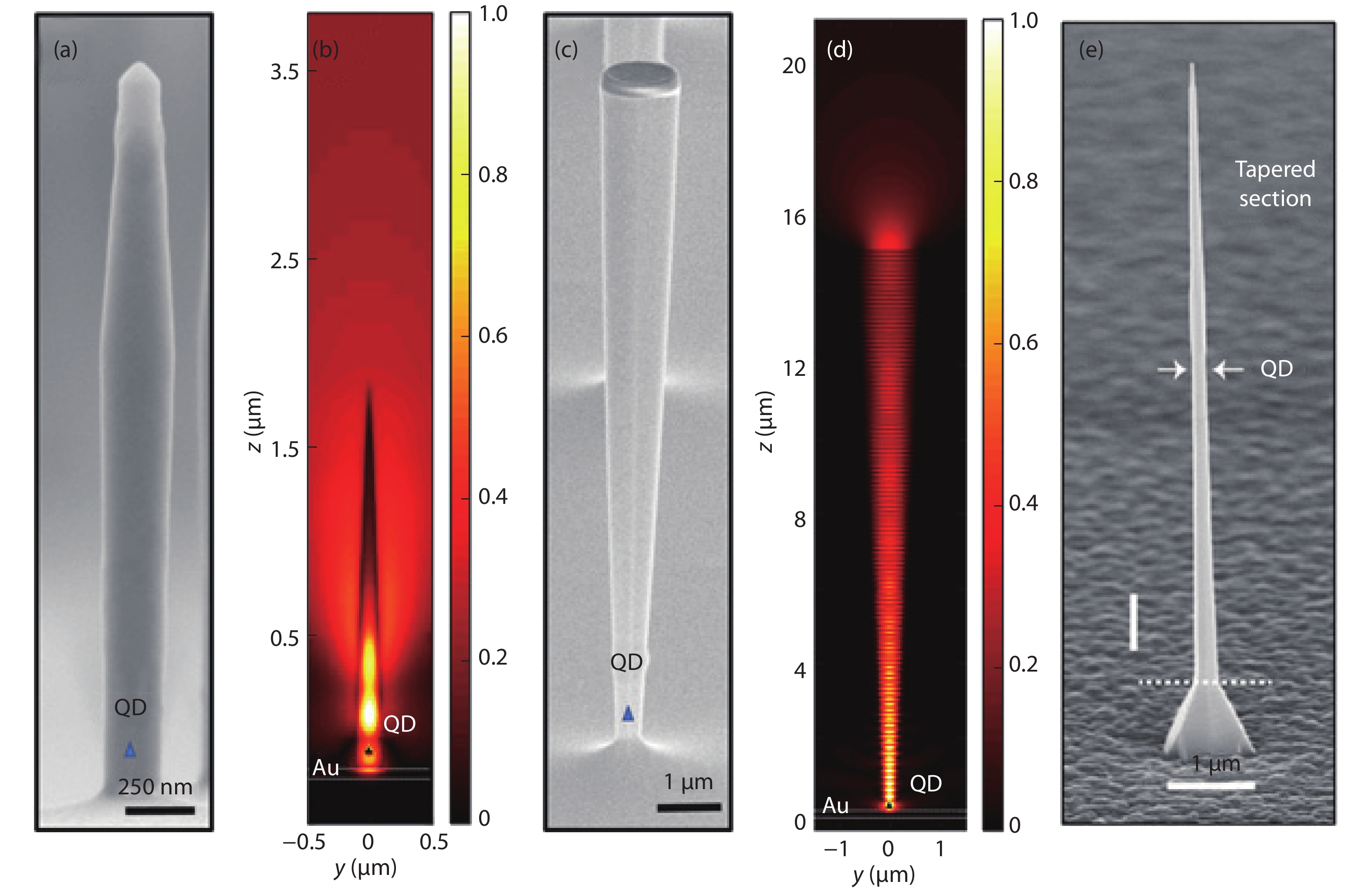
![(Color online) (a–b) Scanning electron microscopy (SEM) image (a) of a top–down tapered GaAs nanowire waveguide with an embedded InAs QD, together with the intensity profile for a 2D-cut along the nanowire growth axis by FDTD simulation (b). (c–d) SEM image (c) of a top–down GaAs photonic trumpet with an embedded InAs QD, together with the intensity profile for a 2D-cut along the nanowire growth axis by FDTD simulation (d). (e) SEM image of a bottom–up tapered InP nanowire waveguide containing a single InAsP QD[51], reprinted with permission, Copyright 2012, Springer Nature.](/richHtml/jos/2019/40/7/071905/img_1.jpg)
Fig. 1. (Color online) (a–b) Scanning electron microscopy (SEM) image (a) of a top–down tapered GaAs nanowire waveguide with an embedded InAs QD, together with the intensity profile for a 2D-cut along the nanowire growth axis by FDTD simulation (b). (c–d) SEM image (c) of a top–down GaAs photonic trumpet with an embedded InAs QD, together with the intensity profile for a 2D-cut along the nanowire growth axis by FDTD simulation (d). (e) SEM image of a bottom–up tapered InP nanowire waveguide containing a single InAsP QD[51 ], reprinted with permission, Copyright 2012, Springer Nature.
![(Color online) (a) Illustration of a finite PCW with a single QD embedded. (b) The band structure and waveguide modes of PCWs. (c) SEM picture of a PCW. (d) Decay dynamics for QDs that couple and uncouple to the PCWs[68], reprinted with permission, Copyright 2014, American Physical Society.](/richHtml/jos/2019/40/7/071905/img_2.jpg)
Fig. 2. (Color online) (a) Illustration of a finite PCW with a single QD embedded. (b) The band structure and waveguide modes of PCWs. (c) SEM picture of a PCW. (d) Decay dynamics for QDs that couple and uncouple to the PCWs[68 ], reprinted with permission, Copyright 2014, American Physical Society.
Fig. 3. (Color online) (a) The dielectric antenna consists of, from bottom to top, a silver layer, an AlGaAs membrane (with embedded QDs), a low refractive index PMMA spacer and the GaP SIL. Most photon emission is funneled into the GaP SIL[70 ], reprinted with permission, Copyright 2018, Springer Nature. (b) Comparison of the photon-extraction efficiency for different micro-lens mirror structures. With DBR bottom mirror, the photon extraction efficiency reaches to a plateau value of only around 23%, while with a gold bottom mirror, it is improved to more than 80% for large numerical aperture collection objectives[71 ], reprinted with permission, Copyright 2015, Springer Nature. (c) Schematic view of the QD micro-lens/micro-objective device. A micro-objective is printed directed on top of a QD micro-lens[73 ], reprinted with permission, Copyright 2017, American Chemical Society.
Fig. 4. (Color online) (a–c) SEM images of CBG structure[7 ], (a–c) are reprinted with permission, Copyright 2011, AIP Publishing. (d) The schematic of the CBR-HBR. (e) Simulated Purcell facor and collection efficiency of the CBR-HBR[3 ], (d) and (e) are reprinted with permission, Copyright 2019, Nature Springer.

Set citation alerts for the article
Please enter your email address


