
Zhe He, Jiawei Yang, Lidan Zhou, Yan Chen, Tianming Zhao, Ying Yu, Jin Liu. Broadband photonic structures for quantum light sources[J]. Journal of Semiconductors, 2019, 40(7): 071905
- Journal of Semiconductors
- Vol. 40, Issue 7, 071905 (2019)
Abstract
1. Introduction
Quantum photonic technologies requires high-performance light sources that emit quantum state of photons on-demand. Semiconductor QDs have been long believed as a very promising system for such high-performance quantum light sources because it can emit one single-photon or one entangled photon pair at a time under external optical/electrical excitations[
Embedding single QDs in photonic nanostructures has been widely explored as a very effective strategy for improving the performance of quantum light sources based on QDs. Last decades have witnessed the tremendous developments on micro-cavities with high quality (Q) factors and small mode volumes in a variety of geometries, e.g., micro-disk[
In this review article, we summarize recently developed broadband photonic nanostructures that are designed for coupling to semiconductor QDs and their applications in high-quality non-classic light generations. The design principle, fabrication process and device performances of the photonic nanowires, photonic crystal waveguides (PCWs), micro-lens and circular Bragg gratings (CBGs) will be discussed in the following.
2. Waveguide-based broadband photonic structures
2.1. Photonic nanowires
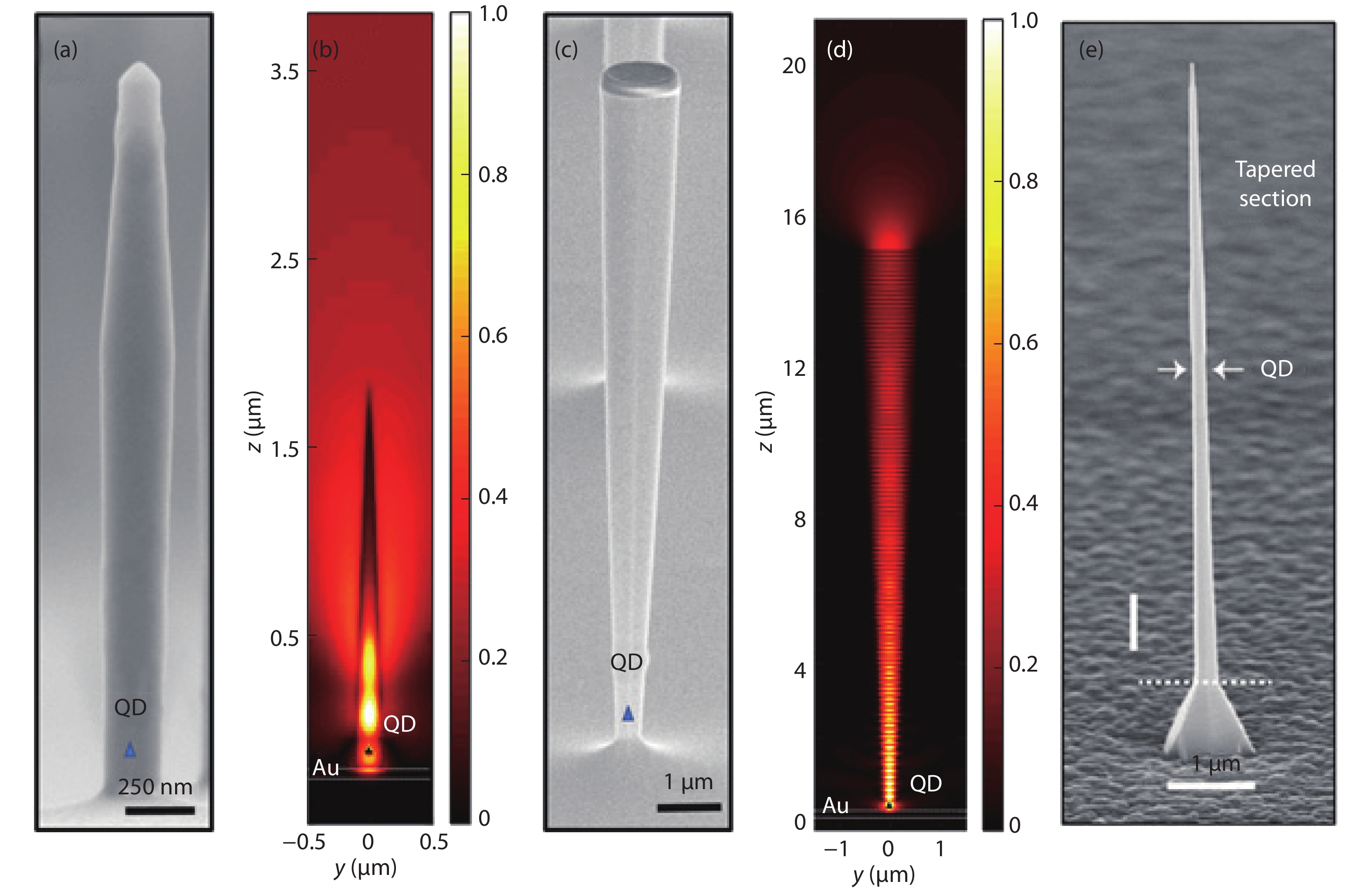
Nanowires were proposed to working as a waveguide because of their considerably enhanced light extraction efficiency along the axial direction. As illustrated in Figs. 1(a) and 1(b), a nanowire with the optimized diameter can efficiently funnel the spontaneous emission from QDs into the fundamental HE11 mode and suppress the coupling to other radiative modes[
![]()
Figure 1.(Color online) (a–b) Scanning electron microscopy (SEM) image (a) of a top–down tapered GaAs nanowire waveguide with an embedded InAs QD, together with the intensity profile for a 2D-cut along the nanowire growth axis by FDTD simulation (b). (c–d) SEM image (c) of a top–down GaAs photonic trumpet with an embedded InAs QD, together with the intensity profile for a 2D-cut along the nanowire growth axis by FDTD simulation (d). (e) SEM image of a bottom–up tapered InP nanowire waveguide containing a single InAsP QD[
Top-down and bottom-up methods are mostly employed to fabricate QD-in-nanowires. The top-down approach is based on epitaxial growth of QD materials combined with plasma dry etching technique[
High symmetry QDs fabricated in the [111] growth direction should exhibit vanishing FSS and, therefore, could emit entangled photon pairs via the biexciton-exciton cascaded radiative process[
Recently, a large static strain tuning of up to 25 meV for a QD embedded in a nanowire trumpet stressed by nanomanipulators[
2.2. Photonic crystal waveguides
Instead of efficiently coupling the quantum light from semiconductor material to the free space optics, PCW serves as a very effective tool of routing the single-photons in the semiconductor chips due to its planar geometry.
The PCs discussed in this work refer to thin semiconductor membranes with periodically etched air holes which create the photonic bandgap for the photons travelling in the membranes (below the light line). The vertical confinement of photons is governed by the total internal reflection between the semiconductor and air interface. The band structure of an infinite PCW is shown in Fig. 2(a). By leaving a line of the air holes, a waveguide mode can be created in the photonic band gap, as illustrated in Fig. 2(b). The solid and dashed lines corresponds to the first and second waveguide modes within the TE-like band gap. The gray shaded area above the light line represents the continuum of radiation modes. A SEM image of a representative PCW device is shown in Fig. 2(c). Interestingly, the density of the optical state of the waveguide modes is greatly enhanced at the band edge, resulting in a pronounced Purcell factor for the QDs that couples to the waveguide modes[
![]()
Figure 2.(Color online) (a) Illustration of a finite PCW with a single QD embedded. (b) The band structure and waveguide modes of PCWs. (c) SEM picture of a PCW. (d) Decay dynamics for QDs that couple and uncouple to the PCWs[
The first unequivocal experimental demonstration of highly efficient broadband coupling of InAs QDs to GaAs PCWs was shown by Hansen et al.[
Despite the impressive beta factors demonstrated in this work, the collection of photons coupling to the propagating waveguide modes was rather inefficient in a confocal micro-PL setup. Only a small portion of photons that couples to the waveguide can be collected by the objective above the waveguides due to some out-of-plane scattering, which results in a very low photon count rates in single-photon detectors. Therefore, it is highly desirable to measure decay rates of QDs that coupled to the PCWs from the end of the waveguides. In the measurements by Laucht et al.[
In addition, QDs with beta > 0.9 were measured across the large spectral range over 20 nm. Although the PCWs funnel the single-photons emitted by QDs to the targeted propagating waveguide modes, the photon count rates in the single-photon detectors is still far from satisfactory. This is mostly due to the mode mismatch between the modes with nanoscale cross-section in the PCWs and the single-mode fiber with a core diameter of a few microns. Such a technical challenge was recently handled by extracting photons in the PCWs via specially prepared tapered fibers. An optical fiber was tapered down to a few hundred nanometers to phase match with the waveguide modes. By deliberately making local minimal height in the tapered fiber and accurately launching to the waveguides regime, ~80% of photons in the waveguide was guided to the fiber with a single-photon count rate up to 4.38 MHz obtained in the single photon detector, corresponding to a source efficiency more than 10% [
3. Lens-based broadband photonic structures
3.1. Solid immersion lens
The most straightforward way to increase the light extraction is to use a lens to guide the emitted photons to the collection optics. For semiconductor QDs, solid immersion lens (SIL) made of high refractive index materials represents a viable option. Zirconia lens is widely employed in enhancing the photon count rate. But compared with the GaAs material, the refractive index of Zirconia is relatively small, leading to an insufficient extraction of QDs photons. Gallium phosphide (GaP) semi-sphere lens (with refractive coefficient similar to GaAs) is recently exploited by Chen and co-workers[
![]()
Figure 3.(Color online) (a) The dielectric antenna consists of, from bottom to top, a silver layer, an AlGaAs membrane (with embedded QDs), a low refractive index PMMA spacer and the GaP SIL. Most photon emission is funneled into the GaP SIL[
3.2. Micro-lens
Despite the simplicity and the effectiveness of the SIL approach, the large footprint of the macroscopic lens prevents the possibility of addressing individual QDs independently. The idea of the lens can be transformed from macroscopic SIL to microscopic lens, i.e., micro-lens.
Similar to SIL, the micro-lens shapes the propagation of the emitted photons, effectively guiding the photons towards the collection lens. With a backside reflector, those photons not caught by the nanostructure can be reflected back to the lens and significantly improve the device performances.
By deterministically placing singe QDs in the micro-lens with a bottom distributed Bragg mirror (DBR), single-photon collection efficiency up to 23% across a broad operation bandwidth is observed (red line in Fig. 3(b))[
4. Cavity based photonic structures: circular Bragg gratings
Apart from generating single-photons, the polarization entangled photon pairs can also be deterministically triggered from semiconductors by using the bi-exciton(XX)/exciton(X) cascaded radiative recombination process. Generally, the X and XX transitions are not frequency-degenerate, resulting in a wavelength separation of X and XX photons for a few nanometers[
One of the clever solutions is to use a low-Q circular Bragg grating (CBG) resonator proposed by Davanco et al.[
![]()
Figure 4.(Color online) (a–c) SEM images of CBG structure[
5. Conclusion
Last decades have witnessed the race of different photonic structures for the realizations of semiconductor quantum light sources. The broadband photonic structures greatly reduce the challenge of spectral resonance between the QDs and the structures which is particularly technically difficult for the high-Q cavities. In addition, the propagating mode feature of the waveguide based structure offers a unique opportunity of routing light in planar chips, facilitating the on-chip integration of multiple functional devices. The unique combination of broadband enhancements of spontaneous emission rate and collection efficiency simultaneously further enables the on-demand generation of non-classic state beyond single-photons, i.e., entangled photon pairs. With further developments of the broadband photonic structures, more advanced quantum photonic experiments could be envisioned in the near future, e.g., two-photon quantum random walking and multi-photon boson sampling etc.
Acknowledgments
This work was supported by National Key R&D Program of China (No. 2018YFA0306100), the National Natural Science Foundations of China (Nos. 11874437,11704424), the Natural Science Foundation of Guangdong Province (Nos. 2018B030311027, 2017A030310004, 2016A030310216) and Guangzhou Science and Technology Project (No. 201805010004). the National Natural Science Foundation of China (No. 60123456).
References
[1] D Huber, M Reindl, l J Aberl et al. Semiconductor quantum dots as an ideal source of polarization-entangled photon pairs on-demand: a review. J Opt, 20, 073002(2018).
[2] Y M He, e Y He, i Y J Wei et al. On-demand semiconductor single-photon source with near-unity indistinguishability. Nat Nanotechnol, 8, 213(2013).
[3] J Liu, u R Su, i Y Wei et al. A solid-state source of strongly entangled photon pairs with high brightness and indistinguishability. Nat Nanotechnol, 14, 586(2019).
[4] P Senellart, n G Solomon, A White. High-performance semiconductor quantum-dot single-photon sources. Nat Nanotechnol, 12, 1026(2017).
[5] L Hanschke, r K A Fischer, S Appel et al. Quantum dot single-photon sources with ultra-low multi-photon probability. npj Quantum Inform, 4, 43(2018).
[6] S Kolatschek, S Hepp, M Sartison et al. Deterministic fabrication of circular Bragg gratings coupled to single quantum emitters via the combination of in-situ optical lithography and electron-beam lithography. J Appl Phys, 125, 045701(2019).
[7] M Davanço, M T Rakher, D Schuh et al. A circular dielectric grating for vertical extraction of single quantum dot emission. Appl Phys Lett, 99, 041102(2011).
[8] W L Barnes, G Björk, J M Gérard et al. Solid-state single photon sources: light collection strategies. Eur Phys J D, 18, 197(2002).
[9] K Srinivasan, M Borselli, n T J Johnson et al. Optical loss and lasing characteristics of high-quality-factor AlGaAs microdisk resonators with embedded quantum dots. Appl Phys Lett, 86, 151106(2005).
[10] K Srinivasan, O Painter. Linear and nonlinear optical spectroscopy of a strongly coupled microdisk–quantum dot system. Nature, 450, 862(2007).
[11] T Zhou, M Tang, G Xiang et al. Ultra-low threshold InAs/GaAs quantum dot microdisk lasers on planar on-axis Si (001) substrates. Optica, 6, 430(2019).
[12] P Michler, A Kiraz, C Becher et al. A quantum dot single-photon turnstile device. Science, 290, 2282(2000).
[13] S Liu, Y Wei, R Su et al. A deterministic quantum dot micropillar single photon source with > 65% extraction efficiency based on fluorescence imaging method. Sci Rep, 7, 13986(2017).
[14] C Böckler, S Reitzenstein, C Kistner et al. Electrically driven high-
[15] T Heindel, C Schneider, M Lermer et al. Electrically driven quantum dot-micropillar single photon source with 34% overall efficiency. Appl Phys Lett, 96, 011107(2010).
[16] C Schneider, P Gold, S Reitzenstein et al. Quantum dot micropillar cavities with quality factors exceeding 250,000. Appl Phys B, 122, 19(2016).
[17] N Somaschi, V Giesz, L De Santis et al. Near-optimal single-photon sources in the solid state. Nat Photonics, 10, 340(2016).
[18] H Wang, n Z C Duan, i Y H Li et al. Near-transform-limited single photons from an efficient solid-state quantum emitter. Phys Rev Lett, 116, 213601(2016).
[19] B Ellis, r M A Mayer, G Shambat et al. Ultralow-threshold electrically pumped quantum-dot photonic-crystal nanocavity laser. Nat Photonics, 5, 297(2011).
[20] Y Gong, B Ellis, G Shambat et al. Nanobeam photonic crystal cavity quantum dot laser. Opt Express, 18, 8781(2010).
[21] J Vučković, Y Yamamoto. Photonic crystal microcavities for cavity quantum electrodynamics with a single quantum dot. Appl Phys Lett, 82, 2374(2003).
[22] K J Hennessy, C P Reese, A Badolato et al. High-
[23] Y Song, M Liu, Y Zhang et al. High-
[24] D Englund, D Fattal, E Waks et al. Controlling the spontaneous emission rate of single quantum dots in a two-dimensional photonic crystal. Phys Rev Lett, 95, 013904(2005).
[25] K Hennessy, A Badolato, M Winger et al. Quantum nature of a strongly coupled single quantum dot-cavity system. Nature, 445, 896(2007).
[26] D J P Ellis, n R M Stevenson, g R J Young et al. Control of fine-structure splitting of individual InAs quantum dots by rapid thermal annealing. Appl Phys Lett, 90, 011907(2007).
[27] W Heller, U Bockelmann, G Abstreiter. Electric-field effects on excitons in quantum dots. Phys Rev B, 57, 6270(1998).
[28] A J Bennett, y M A Pooley, n R M Stevenson et al. Electric-field-induced coherent coupling of the exciton states in a single quantum dot. Nat Physics, 6, 947(2010).
[29] F Schäffler. High-mobility Si and Ge structures. Semicond Sci Technol, 12, 1515(1997).
[30] C Y Hung, T E Schlesinger, d M L Reed. Piezoelectrically induced stress tuning of electro-optic devices. Appl Phys Lett, 59, 3598(1991).
[31] F Ding, R Singh, f J D Plumhof et al. Tuning the exciton binding energies in single self-assembled InGaAs/GaAs quantum dots by piezoelectric-induced biaxial stress. Phys Rev Lett, 104, 067405(2010).
[32]
[33] I Friedler, C Sauvan, n J P Hugonin et al. Solid-state single photon sources: the nanowire antenna. Opt Express, 17, 2095(2009).
[34] J Bleuse, J Claudon, M Creasey et al. Inhibition, enhancement, and control of spontaneous emission in photonic nanowires. Phys Rev Lett, 106, 103601(2011).
[35] I Friedler, P Lalanne, J P Hugonin et al. Efficient photonic mirrors for semiconductor nanowires. Opt Lett, 33, 2635(2008).
[36] N Gregersen, n T R Nielsen, J Claudon et al. Controlling the emission profile of a nanowire with a conical taper. Opt Lett, 33, 1693(2008).
[37] J Claudon, N Gregersen, P Lalanne et al. Harnessing light with photonic nanowires: fundamentals and applications to quantum optics. ChemPhysChem, 14, 2393(2013).
[38] P Stepanov, a A Delga, N Gregersen et al. Highly directive and Gaussian far-field emission from " giant” photonic trumpets. Appl Phys Lett, 107, 141106(2015).
[39] G Bulgarini, r M E Reimer, k M B Bavinck et al. Nanowire waveguides launching single photons in a Gaussian mode for ideal fiber coupling. Nano Lett, 14, 4102(2014).
[40] N Gregersen, D P S McCutcheon, J Mørk et al. A broadband tapered nanocavity for efficient nonclassical light emission. Opt Express, 24, 20904(2016).
[41] T Mårtensson, P Carlberg, M Borgström et al. Nanowire arrays defined by nanoimprint lithography. Nano Lett, 4, 699(2004).
[42] R S Wagner, s W C Ellis. Vapor-liquid-solid mechanism of single crystal growth. Appl Phys Lett, 4, 89(1964).
[43] T Mårtensson, M Borgström, W Seifert et al. Fabrication of individually seeded nanowire arrays by vapour–liquid–solid growth. Nanotechnology, 14, 1255(2003).
[44] Q Gao, D Saxena, F Wang et al. Selective-area epitaxy of pure wurtzite InP nanowires: high quantum efficiency and room-temperature lasing. Nano Lett, 14, 5206(2014).
[45] J Claudon, J Bleuse, k N S Malik et al. A highly efficient single-photon source based on a quantum dot in a photonic nanowire. Nat Photonics, 4, 174(2010).
[46] M Munsch, k N S Malik, E Dupuy et al. Dielectric GaAs antenna ensuring an efficient broadband coupling between an InAs quantum dot and a gaussian optical beam. Phys Rev Lett, 110, 177402(2013).
[47] D Cadeddu, J Teissier, n F R Braakman et al. A fiber-coupled quantum-dot on a photonic tip. Appl Phys Lett, 108, 011112(2016).
[48] I Yeo, P L de Assis, A Gloppe et al. Strain-mediated coupling in a quantum dot-mechanical oscillator hybrid system. Nat Nanotechnol, 9, 106(2013).
[49] M Munsch, n A V Kuhlmann, D Cadeddu et al. Resonant driving of a single photon emitter embedded in a mechanical oscillator. Nat Commun, 8, 76(2017).
[50] S A Fortuna, X Li. Metal-catalyzed semiconductor nanowires: a review on the control of growth directions. Semicond Sci Technol, 25, 024005(2010).
[51] M E Reimer, G Bulgarini, N Akopian et al. Bright single-photon sources in bottom-up tailored nanowires. Nat Commun, 3, 737(2012).
[52] R Singh, G Bester. Nanowire quantum dots as an ideal source of entangled photon pairs. Phys Rev Lett, 103, 063601(2009).
[53] T Huber, A Predojević, M Khoshnegar et al. Polarization entangled photons from quantum dots embedded in nanowires. Nano Lett, 14, 7107(2014).
[54] M A M Versteegh, M E Reimer, K D Jöns et al. Observation of strongly entangled photon pairs from a nanowire quantum dot. Nat Commun, 5, 5298(2014).
[55] Y Chen, I E Zadeh, Jöns K D et al. Controlling the exciton energy of a nanowire quantum dot by strain fields. Appl Phys Lett, 108, 182103(2016).
[56] P Stepanov, M Elzo-Aizarna, J Bleuse et al. Large and uniform optical emission shifts in quantum dots strained along their growth axis. Nano Lett, 16, 3215(2016).
[57] G Sallen, A Tribu, T Aichele et al. Subnanosecond spectral diffusion of a single quantum dot in a nanowire. Phys Rev B, 84, 041405(2011).
[58] M Holmes, S Kako, K Choi et al. Spectral diffusion and its influence on the emission linewidths of site-controlled GaN nanowire quantum dots. Phys Rev B, 92, 115447(2015).
[59] M E Reimer, G Bulgarini, A Fognini et al. Overcoming power broadening of the quantum dot emission in a pure wurtzite nanowire. Phys Rev B, 93, 195316(2016).
[60] I Yeo, k N S Malik, M Munsch et al. Surface effects in a semiconductor photonic nanowire and spectral stability of an embedded single quantum dot. Appl Phys Lett, 99, 233106(2011).
[61] C C Chang, i C Y Chi, M Yao et al. Electrical and optical characterization of surface passivation in GaAs nanowires. Nano Lett, 12, 4484(2012).
[62] M Müller, S Bounouar, K D Jöns et al. On-demand generation of indistinguishable polarization-entangled photon pairs. Nat Photonics, 8, 224(2014).
[63] H Jayakumar, A Predojević, T Huber et al. Deterministic photon pairs and coherent optical control of a single quantum dot. Phys Rev Lett, 110, 135505(2013).
[64] A V Kuhlmann, l J H Prechtel, J Houel et al. Transform-limited single photons from a single quantum dot. Nat Commun, 6, 8204(2015).
[65] V S C M Rao, S Hughes. Single quantum dot spontaneous emission in a finite-size photonic crystal waveguide: proposal for an efficient " on chip” single photon gun. Phys Rev Lett, 99, 193901(2007).
[66] T Lund-Hansen, S Stobbe, B Julsgaard et al. Experimental realization of highly efficient broadband coupling of single quantum dots to a photonic crystal waveguide. Phys Rev Lett, 101, 113903(2008).
[67] A Laucht, S Pütz, T Günthner et al. A waveguide-coupled on-chip single-photon source. Phys Rev X, 2, 011014(2012).
[68] M Arcari, I Söllner, A Javadi et al. Near-unity coupling efficiency of a quantum emitter to a photonic crystal waveguide. Phys Rev Lett, 113, 093603(2014).
[69] R S Daveau, K C Balram, T Pregnolato et al. Efficient fiber-coupled single-photon source based on quantum dots in a photonic-crystal waveguide. Optica, 4, 178(2017).
[70] Y Chen, M Zopf, R Keil et al. Highly-efficient extraction of entangled photons from quantum dots using a broadband optical antenna. Nat Commun, 9, 2994(2018).
[71] M Gschrey, A Thoma, P Schnauber et al. Highly indistinguishable photons from deterministic quantum-dot microlenses utilizing three-dimensional in situ electron-beam lithography. Nat Commun, 6, 7662(2015).
[72] S Fischbach, A Kaganskiy, r E B Y Tauscher et al. Efficient single-photon source based on a deterministically fabricated single quantum dot-microstructure with backside gold mirror. Appl Phys Lett, 111, 011106(2017).
[73] S Fischbach, A Schlehahn, A Thoma et al. Single quantum dot with microlens and 3D-printed micro-objective as integrated bright single-photon source. ACS Photonics, 4, 1327(2017).
[74] A W Schell, J Kaschke, J Fischer et al. Three-dimensional quantum photonic elements based on single nitrogen vacancy-centres in laser-written microstructures. Sci Rep, 3, 1577(2013).
[75] T Gissibl, S Thiele, A Herkommer et al. Two-photon direct laser writing of ultracompact multi-lens objectives. Nat Photonics, 10, 554(2016).
[76] D Huber, M Reindl, Y Huo et al. Highly indistinguishable and strongly entangled photons from symmetric GaAs quantum dots. Nat Commun, 8, 15506(2017).
[77] L Sapienza, M Davanço, A Badolato et al. Nanoscale optical positioning of single quantum dots for bright and pure single-photon emission. Nat Commun, 6, 7833(2015).
[78] H Wang, H Hu, g T H Chung et al. On-demand semiconductor source of entangled photons which simultaneously has high fidelity, efficiency, and indistinguishability. Phys Rev Lett, 122, 113602(2019).


Set citation alerts for the article
Please enter your email address

© Copyright 2018-2021 | Chinese Laser Press. All Rights Reserved 沪ICP备15018463号-20