The electrical nonlinearity of silicon modulators based on reversed PN junctions was found to severely limit the linearity of the modulators. This effect, however, was inadvertently neglected in previous studies. Considering the electrical nonlinearity in simulation, a 32.2 dB degradation in the CDR3 (i.e., the suppression ratio between the fundamental signal and intermodulation distortion) of the modulator was observed at a modulation speed of 12 GHz, and the spurious free dynamic range was simultaneously degraded by 17.4 dB. It was also found that the linearity of the silicon modulator could be improved by reducing the series resistance of the PN junction. The frequency dependence of the linearity due to the electrical nonlinearity was also investigated.
Analog photonic links (APLs) have several advantages, such as wide bandwidths, low losses, and immunity to electromagnetic interference. They are suitable for applications in wireless access, antenna remoting, high-frequency signal generation, and processing [1–4]. In APLs, modulators are key devices that are used to impose RF signals onto the optical carriers [5]. Currently, modulators are commonly used even though they are bulky and expensive, which limits the widespread application of APLs [6]. On the other hand, silicon modulators have emerged over the past decade and now hold promising for a wide variety of APL applications because of their advantages, which include complementary metal oxide semiconductor (CMOS) compatibility, compact size, low cost, and suitability for integration [7]. However, the linearity of silicon modulators, which is a key figure of merit for their applications in APLs, has not been sufficiently explored.
Silicon modulators based on reversed PN junctions are suitable for gigahertz modulation [8,9]. The nonlinearity of these modulators previously studied was generally considered to occur because of two factors: the nonlinear electro-optic effect based on the free carrier dispersion, and the nonlinear response of the optical interferometer [10–16]. However, the electrical nonlinearity (EN) of the reversed PN junction was neglected in previous studies [17]. In this paper, we took the EN into consideration and found that the EN of the PN junction severely limits the linearity of silicon modulators. Consequently, it should be considered during modulator design. It was found that the EN causes the linearity of the silicon modulator to be frequency-dependent, and acts as a dominant nonlinear factor at a high modulation speed. It was also found that the linearity of the silicon modulator can be improved by reducing the series resistance of the PN junction.
2. THEORY
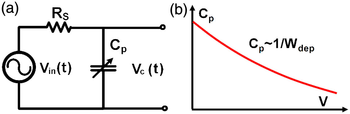
The EN of a silicon modulator originates from its phase shifter, which consists of a reversed PN junction. The equivalent circuit for the reversed PN junction is shown in Fig. 1(a) and it can be simplified into a series connection of a resistance and a depletion capacitor . The depletion capacitance varies with the reverse bias voltage across the PN junction because the depletion width changes with the bias voltage [18], as shown in Fig. 1(b).
Sign up for Photonics Research TOC. Get the latest issue of Photonics Research delivered right to you!Sign up now
Figure 1.(a) Equivalent circuit for the reversed PN junction and (b) relationship between the depletion capacitance and reverse bias voltage.
As shown in Fig. 1(a), the input driving voltage is imposed on the entire PN junction. However, only the voltage on the depletion capacitor contributes to the electro-optic effect. The relationship between and are given by
Here, the PN junction is treated as an abrupt junction in the simulation. Equation (2) shows the approximation of the depletion capacitance for an abrupt junction [18] in which represents the depletion capacitance without a bias voltage and is a constant that is determined by fitting Eq. (2) with the data of the PN junction.
The nonlinear electro-optic response of the silicon phase shifter and the response of the optical interferometer in the silicon modulator can be described using nonlinear power series functions, as given below, in which only the first three power series items are listed. In these functions, and are the phase and absorption changes of the silicon phase shifter, respectively; , , , and are the power series coefficients of the electro-optic response and the response of the optical interferometer, respectively; is the time-varying part of the output power of the silicon modulator. These are the nonlinearities considered in the conventional model [10–16], and are referred to as the power series nonlinearities (PSNs):
With these mathematical expressions, the total nonlinearity of a silicon modulator based on a reversed PN junction can be estimated. Because our model takes the EN into consideration, the total nonlinearity model of the silicon modulator is based on a nonlinear differential equation instead of the traditional power series functions.
3. SIMULATION RESULTS
To study the properties of the EN, we commenced the simulation with a typical 1 mm long phase shifter structure based on a vertical PN junction, whose cross section is plotted in Fig. 2(a). The -type doped concentration was and the -type doped concentration was . The center of the PN junction was aligned 50 nm away from the waveguide center to enhance the electro-optic response. The series resistance of the PN junction was set to a typical value of [19], and was set to be a two-tone signal at and , with a reverse DC bias of 2 V and an RF power of 10 dBm at each frequency. The initial phase of each frequency was zero.
Figure 2.(a) Cross-section of a silicon phase shifter based on a vertical PN junction. (b–d) Calculated nonlinear relationships of the optical phase change, absorption coefficient change, and depletion capacitance versus the different reverse bias voltages and the fitting results.
The phase change, absorption coefficient change, and the depletion capacitance of the phase shifter under different reverse bias voltages were calculated and are displayed in Figs. 2(b)–2(d). The power series coefficients for the electro-optic response, , , were extracted by expanding the fitted nonlinear curves of the phase and absorption coefficient changes into the Taylor series around the DC reverse bias voltage. These curves were fitted using the square root function. Furthermore, and were determined by fitting the simulated data with the abrupt junction approximation described in Eq. (2).
The electrical spectrum of can be obtained by solving Eq. (1) with the harmonic balance method. The calculated spectrum of is illustrated in Fig. 3 in which only the intermodulation distortions (IMDs) at and are considered. The emergence of the IMD indicates that the electrical signal was distorted by the PN junction. It should be noted that the phase difference between the IMD () and the fundamental signal (FUND) (9.8 dBm) was 112.1°.
Figure 3.Simulated spectrum of the EN output : (a) power distribution and (b) phase distribution.
The results in Fig. 3 show that the response of the EN is considerably different from that of the PSNs. For the PSNs in a silicon modulator, as described in Eqs. (3), (4), and (5), the power series coefficient is either a positive or a negative real value; hence, the IMD outputs from the PSNs have either a zero phase difference or a phase difference of 180° with the FUNDs. Thus, the IMD outputs from the PSNs are in phase and can be adjusted to balance each other. However, the IMD output of the EN is clearly out of phase with that of the PSNs. The IMD of the silicon modulator is a combination of the IMDs from the PSNs and the ENs, as shown in Fig. 4. The out-of-phase relationship between the IMDs of the PSNs and the ENs indicates that the IMD of the modulator cannot be perfectly canceled. However, in the conventional nonlinearity model, only the PSNs are considered and the IMD can be canceled.
To better understand the effect of the EN, we investigated a typical Mach–Zander modulator (MZM) with the phase shifter discussed above. As shown in Fig. 5(a), the MZM was single-ended-driven with the two-tone signal described above. On the other arm of the MZM, the optical phase bias between the two arms was adjusted by the thermo-optic phase shifter. When the optical phase bias was varied from , the suppression ratio between the FUND and the IMD (usually denoted as CDR3) of the MZM output was calculated for the conventional nonlinear model without the EN, and for our nonlinear model with the EN, respectively. The results are plotted in Fig. 5(b).
Figure 5.(a) Structure of the simulated MZM, (b) CDR3 under different phase biases for the nonlinear model with EN and the conventional nonlinear model without EN, and (c) SFDR results for the nonlinear model with EN and the conventional nonlinear model without EN.
As can be seen from Fig. 5(b), the CDR3 result for the conventional model without the EN shows a sharp nonlinearity cancellation peak. Nevertheless, when the EN is taken into consideration, the sharp peak vanishes, the curve becomes flat, and there is a degradation of 32.2 dB in the highest CDR3 value. For the model without the EN, the third-order nonlinearity can be canceled when the phase bias of the MZM is . (A detailed explanation can be found in Appendix A.) At this phase bias, the FUND and the IMD under different driving powers were calculated and plotted in Fig. 5(c). The slope of the curve of the IMD versus the driving power was five, indicating that the third-order nonlinearity was fully canceled. A spurious free dynamic range (SFDR) of was obtained in this case. However, when the EN was considered, there was no proper value of the phase bias wherein the third-order nonlinearity could be canceled. For the model with the EN, at the phase bias wherein the CDR3 was the highest, the FUND and the IMD under different driving powers were also calculated and plotted in Fig. 5(c). The slope of the curve of the IMD versus the driving power was three, which indicated that the third-order nonlinearity still existed. The SFDR was only with a 17.4-dB degradation when compared to the model without the EN. These results show that the EN is a critical factor that severely limits the nonlinearity of the silicon modulator. Therefore, the EN cannot be ignored when trying to improve the linearity of the silicon modulator.
The EN is inevitable for a silicon modulator based on the PN junction. However, the impact of the EN can be lessened when the series resistance of the PN junction is reduced. This is because when the series resistance is reduced to zero, the driving voltage is directly applied to the depletion capacitor without electrical distortion. To illustrate this, the highest CDR3 value in scanning of the phase bias of the MZM (denoted as the “optimized CDR3”) was calculated when the series resistance was varied. The results are plotted in Fig. 6(a).
Figure 6.(a) Optimized CDR3 under different series resistances and (b) SFDR when the series resistance is or .
As shown in Fig. 6(a), reducing the series resistance of the PN junction can effectively improve the linearity of the silicon modulator. When was reduced from to , the optimized CDR3 was improved by 18.4 dB. The SFDR was also calculated at the phase bias for the optimized CDR3 when equaled or . It was improved from to with a 5.1 dB improvement when Rs was reduced from to , as shown in Fig. 6(b).
Because the EN originates from the nonlinear RC response, the linearity of the silicon modulator is frequency related. By scanning the driving frequency, the optimized CDR3 of the MZM can be calculated and normalized to the situation where the phase modulation amplitude of the phase shifter is the same. To investigate the influence of the series resistance on the frequency response of the nonlinearity, the normalized CDR3 was calculated for various series resistance values, and the results are plotted in Fig. 7.
Figure 7.Normalized CDR3 versus the driving frequency (the black line shows that the linearity is frequency-independent without EN).
As can be seen in Fig. 7, at a low driving frequency, the model with the EN effect exhibits the same nonlinearity level as the results predicted by the model without the EN. When the frequency increases, the linearity of the silicon modulator degrades significantly. The normalized CDR3 was more than 35 dB lower than the low frequency value for the case with a series resistance of , when the driving frequency was up to 40 GHz. The critical frequency above which the linearity of the silicon modulator degrades significantly is defined as the frequency where the normalized CDR3 falls 3 dB below the low frequency value. Similarly, the critical frequency can be increased by reducing the series resistance. The critical frequency was increased from 0.24 to 2.5 GHz when decreased from to .
4. CONCLUSION
We first considered the EN of the PN junction in the linearity study of the silicon modulator based on the reversed PN junction. In the study, we found that the EN is a critical nonlinear factor and should be considered in the design of silicon modulators. The simulation results of a silicon MZM shows that the EN can severely limit the linearity of the modulator. At a modulation speed of 12 GHz, we observed a degradation of 32.2 dB in the CDR3 and 17.4 dB in the SFDR when the EN was taken into consideration. By reducing the series resistance of the PN junction, the linearity of the silicon modulator can be improved. The calculation results show that when the series resistance of the PN junction was reduced from to , an 18.4 dB improvement in the CDR3 and a 5.1 dB improvement in the SFDR were achieved. In addition, the linearity of the silicon modulator was found to be frequency dependent when the EN was considered. There is a critical frequency above which the linearity of the silicon modulator degrades significantly, and reducing the series resistance can increase the critical frequency.
APPENDIX A
In the conventional nonlinearity model, the transfer function of the MZM can be expressed as given below, where is the optical phase bias between the two arms of the MZM, and and are the absorption and phase changes, respectively, for different drive voltages. The insertion loss of the modulator is neglected, as shown here:
By applying the nonlinear electro-optic relationship in Eqs. (3) and (4) to Eq. (A1) after substituting for , the third nonlinear coefficient of the MZM transfer function can be expressed as
The power series coefficients of the electro-optic response of the silicon phase shifter simulated in this paper are applied in Eq. (A2). The relationship between and is plotted in Fig. 8. It can be seen that at a phase bias of , the third nonlinearity can be eliminated.
Figure 8.Third nonlinear coefficient versus the phase bias.
[8] T. Chu, X. Xiao, H. Xu, X. Li, Z. Li, J. Yu, Y. Yu. High-speed silicon modulators. 39th European Conference and Exhibition on Optical Communication (ECOC), 1-3(2013).