
Chao Zeng, Hua Lu, Dong Mao, Yueqing Du, He Hua, Wei Zhao, Jianlin Zhao. Graphene-empowered dynamic metasurfaces and metadevices[J]. Opto-Electronic Advances, 2022, 5(4): 200098
- Opto-Electronic Advances
- Vol. 5, Issue 4, 200098 (2022)
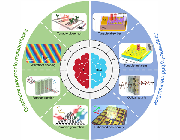
Fig. 1. Overview of state-of-the-art selected functionalities of dynamic metasurfaces and metadevices empowered by graphene. According to the different operation mechanisms, graphene-empowered dynamic metasurfaces are here divided into two classes: graphene plasmonic metasurfaces and graphene-hybrid metasurfaces, each of which holds half the sky. The abbreviations of G and Meta represent graphene and metasurface, and the symbols of A, φ, P, and f stand for the amplitude, phase, polarization, and frequency of EM waves respectively.
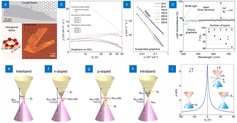
Fig. 2. The basic material properties of graphene. (a ) Micrographs of the scanning electron microscopy (upper panel) and atomic force microscopy (lower right panel), and also a schematic diagram of the 2D hexagonal lattice of graphene (lower left panel). Typical carrier mobility for (b ) graphene on SiO2 with gate-voltage dependence at room temperature and (c ) suspended graphene depending on carrier density at the different temperatures. (d ) Measured transmission spectrum of graphene in the visible range, where the inset is the transmittance as a function of the number of graphene layers. The band structures and its possible transition process for: (e ) pristine or undoped, (f ) n-doped, (g ) p-doped graphene, and (h ) plasmon absorption in n-doped graphene. (i ) Dynamic resistivity ρ with gate voltage Vg applied on graphene, in which the insets show the corresponding position of the Fermi energy EF with changing Vg. Figure reproduced with permission from: (a, i) ref.130, © 2007 Springer Nature; (b) ref.142, © 2008 Springer Nature; (c) ref.144, © 2008 Springer Nature; (d) ref.151, © 2008 AAAS; (e–h) ref.118, © 2012 ACS.
Fig. 3. Polaritons in 2D materials with different dielectric functions and electric field line distributions. (a ) Plasmon-polariton, (b ) phonon-polariton, and (c ) exciton-polariton. The symbol ε1 represents the real part of permittivity, ε2 imaginary part, and ω angular frequency of light. Figure reproduced with permission from ref.171, © 2017 Springer Nature.
Fig. 4. The pioneering experiments on GPs. Tunable THz metamaterials based on the gated graphene microribbon array: (a ) top-view and side-view illustrations of a typical graphene microribbon array on a Si/SiO2 substrate with ion-gel top gate, (b ) transmission spectra of a graphene microribbon array as gate voltage (the inset: AFM image). Tunable infrared plasmonic devices using the stacked graphene/insulator array: (c ) schematic diagram and (d ) SEM image of the stacked graphene/insulator microdisk array, (e ) extinction spectra for different layer numbers of disks, (f ) extinction spectra of a tunable THz linear polarizer using a stacked graphene/insulator microribbon array. (g ) Transmission spectra of graphene on SiC substrate with defects under different magnetic fields. (h ) Extinction spectrum of the edge and bulk plasmon modes and (i ) their corresponding illustration of charged carrier motions. Real-space imaging of GPs: (j ) diagram of infrared nano-imaging experiment and images of plasmon field amplitude, (k ) field amplitude perpendicular to the graphene edge and (l ) plasmon wavelength as the function of gate voltage (the inset: back-gate bias set-up), (m ) near-field optical images of graphene ribbon and tapered graphene ribbon with different wavelengths of excitation light. Figure reproduced with permission from: (a, b) ref.177, © 2011 Springer Nature; (c–f) ref.206, © 2012 Springer Nature; (g) ref.207, © 2012 ACS; (h, i) ref.208, © 2012 ACS; (j–l) ref.210, © 2012 Springer Nature; (m) ref.209, © 2012 Springer Nature.
Fig. 5. Schematic diagrams of a dielectric-graphene-dielectric waveguide and the EM components of the possible TM as well as TE GP modes. β denotes the propagation constant of GPs, ε1 and ε2 represent the relative permittivity of dielectrics below and above graphene sheet, respectively.
Fig. 6. Fundamental properties of TM and TE GPs in an air-graphene-air waveguide. (a ) Dispersion relation and field confinement of TM and TE GPs as the function of Fermi energy calculated from Eqs. (12) and (14) in the MIR~THz regime. (b ) Field confinement comparison between graphene and gold waveguide using the model in Fig. 5 with the same geometric parameters.
Fig. 7. Theoretical models and numerical results for manipulating the energy flow of propagating GPs on 2D plane of graphene sheet by spatially modulating the surface conductivity of graphene. Schematic diagram of the parallel capacitor model with (a ) uneven ground plate Si (h1≠h2) and (b ) nonuniform spacer for example differently doped SiO2 (ε1≠ε2). (c ) Simulated propagation of GPs on a graphene sheet with different bias voltages (Vb1 corresponds to Im(σg)>0 andVb2 corresponds to Im(σg)<0). (d ) Simulated results of graphene-based 2D waveguide using the model in (a). Figure reproduced with permission from: (c, d) ref.211, © 2011 AAAS.
Fig. 8. Schematic model of reflection and refraction of p-polarized light passing through a dielectric-graphene-dielectric interface. The annotated parameters represent: n1 (ε1) and n2 (ε2) the refractive indices (permittivities) of dielectric 1 and 2; θ1 and θ2 the angles of incidence/reflection and refraction; E i, E r, and E t the amplitudes of incident, reflected, and transmitted electric fields; n the normal direction.
Fig. 9. Calculated dynamic transmission and reflection of light due to the GPRs in graphene nanoribbon array according to Eq. (20) . The width of graphene nanoribbon is ~100-nm-scale along x axis and infinite along y axis. The incident light is linearly polarized along x axis.
Fig. 10. Dynamic modulation of the resonance spectra using GP metasurfaces consisting of various localized plasmon resonant structures. (a ) Graphene ribbon: schematic illustration of the device, transmission spectra with different number of graphene layers, arrays with back gate, passive (with ribbon width) and active (with Fermi energy) tunings of plasmon resonance wavelength. (b ) Graphene ring: extinction area in graphene rings with symmetric and anti-symmetric structures. (c ) Graphene disk and ring: scheme of the device consisting of graphene nanodisk array, SEM image of the sample, extinction spectra of graphene nanodisks with different Fermi levels and of graphene nanorings with different outer diameters. (d ) Graphene split-ring: schematic diagram, simulated on-resonance induced current distribution, comparisons of confinement, quality factor, and the ratio of magnetic polarizability density with varying Fermi level. (e ) Graphene nanohole: schematic of the device, measured extinction spectra as a function of gate voltage. (f ) Graphene with 2D conductivity modulation: schematic of the metaatom, simulated transmission and absorption spectra. Figure reproduced with permission from: (a) ref.170, © 2013 AIP Publishing; (b) ref.265, © 2012 AIP Publishing; (c) ref.167, © 2013 ACS; (d) ref.253, Creative Commons Attribution-NonCommercial-Share Alike 3.0 Unported License; (e) ref.267, © 2018 ACS; (f) ref.268, © 2018 ACS.
Fig. 11. Tunable biosensors of vibrational fingerprints using GP metasurfaces based on electrically-tunable spectra of GPRs. Detection of the vibrational fingerprints of proteins: (a ) conceptual view of the sensor based on electrostatically-gated graphene nanoribbon arrays, (b ) measured and calculated extinction spectra for varying bias voltage Vg and corresponding Fermi energy EF. Detection of the vibrational fingerprints and position on the sensor surface of molecules: (c ) schematic diagram of the sensor with pixeled graphene nanodisk arrays and subarrays, (d ) absorption cross-section and (e ) its variation as a function of the active pixel (position). Figure reproduced with permission from: (a, b) ref.272, © 2015 AAAS; (c–e) ref.273, © 2017 ACS.
Fig. 12. Coupling-induced dynamic spectrum modulation with the tunable EIT features using GP metasurfaces. Near-field-coupled graphene nanostrips: (a ) schematic model, (b ) transmission spectra and plasmon mode distribution with varying coupling distances, (c ) transmission spectra as a function of Fermi energy for coupling distances of s=0 and 12 nm. Phase-coupled graphene ribbons: (d ) schematic configuration and transfer matrix model, (e ) transmission dependence on different separations h, (f ) demonstration of electro-optical switch based on the graphene metasurface. Figure reproduced with permission from: (a–c) ref.278, © 2013 AIP Publishing; (d–f) ref.248, © 2014 AIP Publishing.
Fig. 13. Dynamic wavefront shaping using GP metasurfaces based on resonance phase. (a ) Scattering amplitude and phase as the function of Fermi level of the unit cell with two graphene nanoribbon. FP cavity-enhanced graphene metasurface: (b ) schematic of metasurfaces, (c ) reflectivity and phase of the reflected light as a function of ribbon width, (d ) focusing performance at different Fermi levels. Dual-band light focusing reflector using stacked graphene nanoribbon metasurfaces: (e ) schematic model, (f ) amplitude and phase responses of the reflected light, (g ) the relative electric field distributions at resonant frequencies of 15.8 and 25.4 THz, (h ) simulated performances of the dual-band focusing reflector. Figure reproduced with permission from: (a) ref.285, © 2014 John Wiley and Sons; (b–d) ref.286, Creative Commons Attribution 4.0 International License; (e–h) ref.288, © 2017 ACS.
Fig. 14. Dynamic wavefront shaping using GP metasurfaces based on PB phase. Transmission-type graphene nanocrosses metasurface: (a ) schematic model, (b ) transmission amplitude and phase profiles of the CP light at the frequency of 17 THz. Reflection-type graphene nanocrosses metasurface: (c ) reflective phase shifts and simulated phase distributions of three different arrangements (C1, C2, and C3), (d ) phase distributions, interferograms, and far-field electric distributions for 1-order, 3-order, and 15-order vortex-beam-generating metasurfaces. The spin-dependent flat lens: (e ) schematic of the flat lens metasurface, (f ) electric field map under RCP incidence, (g ) electric field map under LCP incidence. Figure reproduced with permission from: (a, b) ref.77, © 2015 John Wiley and Sons; (c, d) ref.122, © 2018 John Wiley and Sons; (e–g) ref.293, © 2019 OSA, under the terms of the OSA Open Access Publishing Agreement.
Fig. 15. Dynamic polarization rotation in graphene metasurfaces based on the magnetoplasmon-enhanced Faraday effects. Graphene microribbon array: (a ) schematic Faraday rotation, (b ) Faraday rotation and (c ) transmission spectra of ribbon arrays and continuous graphene on top of the substrate (ε=4) with relaxation time τ=0.1 ps at various magnetic fields. Equivalent graphene nanodisk array (by spatially modulating conductivity): (d ) schematic far-field Faraday rotation, (e ) Faraday rotation angle and (f ) circular dichroism versus magnetic field at the frequency of 42.7 THz. (f) Measured and simulated Faraday rotation spectra of graphene square antidot (GSA) array at different magnetic fields (the inset: SEM pictures of GSA). (g ) Schematic model and (h ) Faraday rotation spectrum of the graphene micro-ribbon metasurface for normally incident THz pulses at different external magnetic fields. Figure reproduced with permission from: (a–c) ref.296, © 2013 ACS; (d, e) ref.297, © 2014 ACS; (f) ref.298, © 2018 APS; (g, h) ref.299, © 2020 AIP Publishing.
Fig. 16. Dynamic polarization conversion in GP metasurfaces based on polarization-dependent plasmon resonances. Asymmetric graphene nanocrosses metasurfaces: (a ) transmission coefficients and phase difference excited by linearly polarized light, (b ) transmission amplitude ratio, phase difference, rotated polarization angle, and ellipticity versus the incident polarization angle at three wavelengths. (c ) L-shaped graphene nanostructures. (d ) Rectangular graphene patches. (e ) The operation principle of the polarization converter based on crossed-graphene ribbon gratings. Figure reproduced with permission from: (a, b) ref.300, © 2013 OSA, under the terms of the OSA Open Access Publishing Agreement; (c) ref.301, © 2013 AIP Publishing; (d) ref.302, © 2016 OSA; (e) ref.304, © 2018 OSA, under the terms of the OSA Open Access Publishing Agreement.
Fig. 17. Dynamic nonlinear frequency conversion using GP metasurfaces. Harmonic generation in the armchair-edged triangular graphene nanoislands: (a ) illustration of nanoisland and harmonic generation, (b ) time-varying graphene dipole induced by the electric field of incident pulse, (c ) excitation of harmonics for incident pulses with polarizations along the x and y directions. Topologically protected FWM interactions in a specific graphene metasurface: (d ) configuration of a periodic nanohole array in a graphene sheet and FWM of topologically protected one-way edge plasmons, near-field profiles at the frequencies of signal (e ) and idler (f ). Figure reproduced with permission from: (a–c) ref.305, © 2014 Springer Nature; (d–f) ref.127, © 2020 The authors, under a Creative Commons Attribution License 4.0 (CC BY).
Fig. 18. Dynamic trapping and focusing of GP waves propagating along the 2D plane of graphene sheet using GP metasurfaces. GP metasurface with a groove grating silicon as the ground plate of the parallel capacitor: (a ) schematic model with a graded grating silicon plate, (b ) electric fields of GP waves for different wavelengths. GP metasurface with PC-like dielectric layer underneath graphene sheet: (c ) fundamental structure model, field distributions of Maxwell’s Fisheye lens (d ), Luneburg lens (e ), self-focusing lens (f ), and Luneburg lens at different gate voltages (g ) and (h ). Figure reproduced with permission from: (a, b) ref.312, 2015, (c–h) ref.263, 2014, under a Creative Commons Attribution 4.0 International License.
Fig. 19. Dynamic guiding of GP waves propagating along the 2D plane of graphene sheet using GP metasurfaces. GP metasurface with patterned substrate underneath a fully encapsulated graphene sheet: (a ) schematic configuration, (b ) schematic metasurface with an engineered domain wall, (c ) calculated plasmonic band structure, (d ) experimental near-field images at different gate voltages. GP metasurface with periodically patterned air nanoholes in a graphene sheet: (e ) schematic of GP metasurface waveguide by mirror-symmetrically putting two optimized GP metasurfaces together, unidirectional mode propagations of RCP (f ) and LCP light (g ), backscattering-immune propagations in U-, C-, and L-bend domain-wall interfaces (h ). Figure reproduced with permission from: (a–d) ref.314, 2019, under a Creative Commons Attribution 4.0 International License; (e–h) ref.315, © 2020 IEEE.
Fig. 20. Dynamic spectrum modulations using graphene-hybrid metasurfaces. Ultrathin MIR amplitude modulators based on electrically tunable metasurface perfect absorber: (a ) schematic of metasurface modulator comprising plasmonic structures on graphene, (b ) measured reflection spectra for different gate voltages (inset: SEM image of the metasurface on graphene). Electrical modulation of Fano resonance in plasmonic metasurface using graphene: (c ) schematic illustration of the Fano resonant metasurface fabricated on top of graphene with Si back gate, (d ) measured reflectance spectra of the metasurface with ion-gel top electrolyte at different gate voltages. Electrically tunable EIT and slow light using diatomic metasurface integrated with a gated graphene: (e ) schematic view of gate-controlled EIT metasurface, (f ) measured transmission spectra as a function of gate voltage variation. Hybrid graphene metasurfaces for SLM: (g ) schematic of the metasurface, (h ) SEM image, (i ) reflection change and modulation depth as functions of wavelength at gate biases of 7 V (red curve) and -3 V (blue curve), (j ) modulation speed (inset: measurement system) of the SLM, (k ) optical micrograph of 6×6 functional pixels, (l ) photograph of the device, (m ) spatial reflection patterns of “CINT” by selectively applying gate voltages to individual pixels. Figure reproduced with permission from: (a, b) ref.75, © 2014 ACS; (c, d) ref.332, © 2014 ACS; (e, f) ref.335, © 2018 ACS; (g–m) ref.337, under a Creative Commons Attribution 4.0 International License.
Fig. 21. Dynamic wavefront control using graphene-hybrid metasurfaces. Electrically modulation of anomalously refracted THz waves with gated-graphene metasurfaces: (a ) schematic view of the crosspolarized transmission in graphene metasurfaces consisting of a graphene sheet deposited on the array of U-shaped apertures (inset: optical micrograph image), (b ) schematic of the metasurface with linear phase variation and the simulated wavefront control for LCP incidence at different gate voltages, (c ) metasurface with parabolic phase profile for focusing THz waves, (d ) electrically modulations of electric field and energy density of focusing performances. Graphene-enabled electrically controlled THz metalens: (e ) schematic of the active THz metalens composed of an Au metasurface and a graphene layer, (f ) SEM micrograph of the fabricated metalens, (g ) phase distributions of metalens with focal lengths of 7 mm and 9 mm and their phase difference, (h ) length L and (i ) rotation angle θ distributions of the metalens, (j ) and (k ) far-field intensity distributions of the transmitted RCP THz waves at gate voltages of 0 and 2 V respectively. Figure reproduced with permission from: (a–d) ref.343, © 2017 Wiley; (e–k) ref.344, © 2018 Chinese Laser Press.
Fig. 22. Dynamic polarization control using graphene-hybrid metasurfaces. Mid-infrared optical polarization encoding using graphene-integrated plasmonic metasurfaces: (a ) schematic illustration of the polarization encoding process based on the circular orthogonal polarization basis, (b ) and (c ) reflection and normalized Stokes parameter S3 spectra at different gate voltages as functions of wavelength, (d -f ) polarization states of the reflected light under linearly polarized incident light at three different gate voltages, (g ) normalized Stokes parameters (S1, S2, S3) as a function of gate voltage, (h ) corresponding polarization states on the Poincaré sphere, (i ) schematic illustration of the PDM technique realized by the proposed metadevice. Electrical tuning of the polarization state of THz waves using graphene chiral metasurfaces: (j ) schematic rendering of the conjugated double Z metasurface with the ion-gel gate, (k ) and (l ) electric field distributions for RCP and LCP in the metasurfaces at the frequency of 1.1 THz at gate voltages of 0 and 1.8 V respectively, (m ) schematic of CD transmission, (n ) measured transmission spectra for RCP and LCP waves at different gate voltages, (o ) measured and simulated intensity modulation depth as a function of gate voltage (inset: measured CD with different gate voltages), (p ) schematic of OA transmission, (q ) measured ellipticity with different gate voltages, (r ) azimuthal rotation angle θ at the frequency where η=0 as a function of gate voltage. Figure reproduced with permission from: (a–i) ref.348, © 2016 John Wiley and Sons; (j–r) ref.349, under a Creative Commons Attribution NonCommercial License 4.0 (CC BY-NC).
Fig. 23. Electrically reconfigurable digital graphene-hybrid metadevices with spatially varying dielectric constant. (a ) Schematic of a digital metasurface with individually addressable pixels, (b ) and (c ) calculated real and imaginary part of the effective dielectric constant in a single pixel as functions of bias voltages, (d ) schematic of the pixelated metadevice, (e ) and (f ) spatial maps of the real part of the dielectric constant at different voltage configuration, (g ) photograph of fabricated metadevice with 4×4 arrays of active pixel containing 3×3 SRRs, (h ) and (i ) measured transmission patterns corresponding to (e) and (f) respectively. Figure reproduced with permission from ref.79, under a Creative Commons Attribution NonCommercial License 4.0 (CC BY-NC).
Fig. 24. Programmable graphene-hybrid metasurfaces for dynamic wavefront control. (a ) Conceptual illustration of the metasurface, (b ) phase of the reflected waves from the coding graphene metasurface elements, (c ) photograph of fabricated metasurfaces, (d ) measurement system, (e -g ) calculated, simulated, and measured far-field results for beam redirecting at the coding sequence of...0000000011111111..., (h -j ) results for beam redirecting at the coding sequence of...0000111100001111..., (k -m ) results for RCS reduction at the coding sequence of 001011 with 8 unit cells in a lattice, (n -p ) results for RCS reduction at the coding sequence of 001001110101 with 4 unit cells in a lattice. Figure reproduced with permission from ref.353, © 2020 ACS.
Fig. 25. Dynamic scattering steering using graphene-integrated digital coding metasurfaces. (a ) 3D schematic of the metaatom consisting of five layers: graphene layer, spacer, metal pattern, substrate, and ground layer, (b ) optimal coding distributions of the proposed metasurface, (c ) and (d ) photograph of metal patterned layer and graphene patterned layer, (e -g ) simulated 3D scattering patterns at different surface resistances of graphene, (h -m ) measured bistatic RCS of the proposed coding metasurface in the H- and E-plane. Figure reproduced with permission from ref.354, © 2020 John Wiley and Sons.

Set citation alerts for the article
Please enter your email address
© Copyright 2018-2021 | Chinese Laser Press. All Rights Reserved 沪ICP备15018463号-20