1MOE Key Laboratory of Material Physics and Chemistry under Extraordinary Conditions, and Shaanxi Key Laboratory of Optical Information Technology, School of Physical Science and Technology, Northwestern Polytechnical University, Xi’an 710129, China
2State Key Laboratory of Transient Optics and Photonics, Xi’an Institute of Optics and Precision Mechanics, Chinese Academy of Sciences, Xi’an 710119, China
Metasurfaces, with extremely exotic capabilities to manipulate electromagnetic (EM) waves, have derived a plethora of advanced metadevices with intriguing functionalities. Tremendous endeavors have been mainly devoted to the static metasurfaces and metadevices, where the functionalities cannot be actively tuned in situ post-fabrication. Due to the intrinsic advantage of active tunability by external stimulus, graphene has been successively demonstrated as a favorable candidate to empower metasurfaces with remarkably dynamic tunability, and their recent advances are propelling the EM wave manipulations to a new height: from static to dynamic. Here, we review the recent progress on dynamic metasurfaces and metadevices enabled by graphene with the focus on electrically-controlled dynamic manipulation of the EM waves covering the mid-infrared, terahertz, and microwave regimes. The fundamentals of graphene, including basic material properties and plasmons, are first discussed. Then, graphene-empowered dynamic metasurfaces and metadevices are divided into two categories, i.e., metasurfaces with building blocks of structured graphene and hybrid metasurfaces integrated with graphene, and their recent advances in dynamic spectrum manipulation, wavefront shaping, polarization control, and frequency conversion in near/far fields and global/local ways are elaborated. In the end, we summarize the progress, outline the remaining challenges, and prospect the potential future developments.
Introduction
Metasurfaces, artificial subwavelength structured interfaces, exhibit unprecedented capabilities to manipulate electromagnetic (EM) waves ranging from visible to terahertz (THz) and microwave frequencies1-8. By precisely managing the geometric size, orientation, and arrangement of each metaatom in metasurfaces, one can control the amplitude, phase, polarization, and/or frequency of EM waves on demand9-14. In the past decade, this fascinating area has undergone rapid developments, and a plethora of advanced metadevices with outstanding functionalities have been exploited including diffraction-limited focusing15-21, holography22-26, structured light generation27-29, orbital-angular momentum multiplexing/demultiplexing30, 31, and dispersion engineering32-35. It is noteworthy that besides the intriguing functionalities, the natural instinct to miniaturize traditional devices and systems is the ultimate motive force to the development of metasurfaces and metadevices in terms of engineering and industrial applications36. In pace with increasingly powerful micro/nano-fabrication technologies37-41, various functionalized metasurfaces have been integrated on fiber facets42, and into semiconductor43, solid-state44 as well as fiber lasers45, infusing new life and capabilities into the traditional nanodevices. Currently, multi-functional and multi-dimensional metasurfaces are arousing a period of revolution in both traditional and emerging application fields46-48, such as integrated photonics49, 50, nonlinear optics51, 52, next-generation communications53, 54, artificial intelligences55, 56, and quantum technologies57, 58.
Due to the passive nature of building blocks in general made of metals and/or dielectrics, however, aforementioned metasurfaces and metadevices mainly work at static, which means their functionalities cannot be actively tuned in situ after fabrication. There is no doubt, such static feature leads to a fall-off in the functionality of dynamical manipulations and seriously impedes their application scenarios, where dynamic EM wave manipulations are highly desired59-63, for example, varifocal lens64, dynamic holography65, and beam steering in LiDAR system66. Motivated by those significant requirements, scientists have struggled for years to improve the dynamical tunability of metasurfaces, and introducing active materials or components into the passive metasurfaces has been proposed as the first thought strategy. Up to now, various active materials and components such as transparent conducting oxides67-69, phase-change materials70-73, 2D materials (particularly graphene)74-79, varactor diodes80-83, elastic materials84-86, and micro-electro-mechanical system87-89, have been demonstrated theoretically and experimentally to empower the active tunability to metasurfaces and metadevices by applying external thermal, electrical, optical, and mechanical stimulus, giving rise to a new direction, i.e., dynamic (e.g. tunable, reconfigurable, programable, intelligent, and digital coding) metasurfaces and metadevices90-96. It should be noted that although previous researches provide a major source of inspiration for dynamic metasurfaces and metadevices, each type of active materials and components holds a set of unique characteristics, provides encouraging opportunities, and also suffers from different limitations as well as challenges. Several excellent review articles published in recent years have focused on this area to discuss the aforementioned issues97-101. However, a comprehensive review on graphene-based dynamic metasurfaces and metadevices is still absent, which are of equal and even more significance due to the extraordinary properties of graphene.
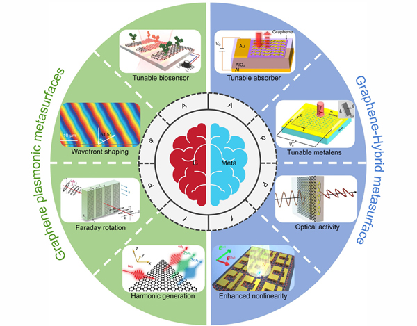
Recent years have witnessed the explosive developments of 2D materials-based electronics and photonics with increasing maturity of preparation and fabrication techniques102-115. Although the family of 2D materials goes from strength to strength, graphene is recognized all the time as one of the most powerful 2D materials due to its intrinsic advantages of active tunability by external stimulus (especially by electrical basis)116, enhanced wave-matter interactions117, ultrabroadband response118, and CMOS-compatibility113. Currently, the combination of the two exciting research fields, i.e., 2D materials and metasurfaces, is propelling the metasurfaces and metadevices to new heights: multifunctionality together with tunability. Thereinto, graphene has been so far the most attractive candidate to exploit dynamic metasurfaces and metadevices with different mechanisms, configurations, and functionalities in the mid-infrared (MIR), THz, and microwave regimes, which can be categorized into two classes: metasurfaces with building blocks of structured graphene and hybrid metasurfaces integrated with graphene74-79, 119-127. The former is called graphene plasmonic metasurfaces and the latter graphene-hybrid metasurfaces (as shown in Fig. 1). Considering the rapid advances of this overlapped field, this review is devoted to the dynamic metasurfaces and metadevices enabled by graphene with an emphasis primarily on electrically-controlled EM wave manipulations in the MIR, THz, and microwave regimes. In Section Fundamentals of graphene, the basic material properties of graphene and plasmons in graphene are introduced, and further the theoretical and numerical models of graphene plasmons are discussed in detail. Then, the state-of-the-art advancements in graphene plasmonic metasurfaces and graphene-hybrid metasurfaces for dynamic spectrum manipulation, wavefront shaping, polarization control, and frequency conversion in near/far fields and global/local ways are highlighted in Sections Metasurfaces with building blocks of structured graphene and Hybrid metasurfaces integrated with graphene. In the end, Section Conclusion and outlook summarizes the progresses, concludes the remaining challenges, and outlooks the potential future developments.
Figure 1.Overview of state-of-the-art selected functionalities of dynamic metasurfaces and metadevices empowered by graphene. According to the different operation mechanisms, graphene-empowered dynamic metasurfaces are here divided into two classes: graphene plasmonic metasurfaces and graphene-hybrid metasurfaces, each of which holds half the sky. The abbreviations of G and Meta represent graphene and metasurface, and the symbols of A, φ, P, and f stand for the amplitude, phase, polarization, and frequency of EM waves respectively.
In 2004, Novoselov and Geim et al. successfully prepared the single-layer graphene from highly oriented pyrolytic graphite by mechanical exfoliation and demonstrated a field-effect transistor using high-quality few-layer graphene, which lifted the curtain of research on 2D materials128-131. The Nobel Prize for Physics in 2010 publicized widely this powerful one-atomic-thick material and also the simple preparation method of mechanical exfoliation, providing the easy access to prepare high-quality graphene, which is now the most popular method, particularly in the photonics and optoelectronics. Since then, 2D materials with the structure and properties similar to graphene, such as black phosphorus (BP)132-134 and transition metal dichalcogenides (TMDCs)135-137, began to gather increasing attention of scientists in the multidisciplinary field, especially in the photonic and optoelectronic community due to their exceptional electrical and optical properties108, 138. Although the family of 2D materials is rather plentiful, due to the easy preparation of remarkably high-quality graphene, flexibly electrical tunability, and CMOS-compatible with silicon photonics, graphene is still one of the most powerful 2D materials for developing high-performance nanodevices including metadevices, where the qualities of 2D materials are critically important, for instance, the mobility, conductivity, defect, size, and layer number114, 139, 140. In this Section, we centre upon graphene to discuss its basic material properties and plasmon mode, and provide the theoretical and numerical models of graphene plasmons. It should be noted that graphene in general represents the single-layer graphene throughout this review if there is no special description.
Basic material properties of graphene
It is well-known that due to its unique electronic structure, graphene has been hailed as a wonderful material with distinctive properties, which provide new solutions to integrated electronics and photonics with the compact footprint, remarkably electrical tunability, broadband and high-speed operation.
(i) One-atomic-scale thickness. Graphene is a single-layer atomic crystal of hexagonally-arranged sp2-hybridized carbon atoms with the lattice constant of ~0.142 nm128. As shown in Fig. 2(a), the thickness of single-layer graphene is one-atomic-scale with the value of ~0.334 nm theoretically and ~0.4 nm experimentally, and the continuous size of high-quality graphene sheet can be up to a macroscopic scale (~100 μm) by using micromechanical exfoliation, which is sufficient for most researches in photonics and optoelectronics130, 141. For the purpose of integration with electronic and photonic platforms, the one-atomic-scale thickness as well as macroscopic-scale size of graphene make it more compatible with CMOS processing at the wafer scale.
(ii) Ultra-high intrinsic carrier mobility. The linear energy-momentum dispersion near the Dirac point renders electrons in graphene travelling at a constant velocity of 3×10⁶ m/s (only 100 times smaller than the light speed, defined as the Fermi velocity), which means the carrier mobility can be ultra-high and thus graphene is an excellent conductor of electricity. It should be pointed out that the mobility can also remain high even when the carrier density is zero at the Dirac point, which is quietly different from semiconductors where carriers become immobile at low density. Although the environment (particular the substrate) significantly affects the mobility of graphene in practice, the experimentally measured mobility is still high enough, for example, ~4×104 cm2V−1s−1 on SiO2 substrate (Fig. 2(b))142, ~1.4×105 cm2V−1s−1 encapsulated within hexagonal boron nitride (hBN) layers143, and ~2×105 cm2V−1s−1 in suspended graphene (Fig. 2(c))144. This implies that graphene-based electronics and optoelectronics have the potential to operate at speed of a few hundred GHz and even to THz, for example, graphene-based modulators145-147 and photodetectors148-150.
(iii) Tunable and broadband responses. Due to the unique electronic band structure that conic-shaped conduction band and valence band meet at the Dirac point, the optical conductance of pristine graphene is frequency-independent and only determined by its fine-structure constant α=e2/ћc≈1/137 (here e is the electron charge, ћ the reduced Planck’s constant, and c the light speed in the vacuum), which directly results in a frequency-independent optical absorption A=πα~2.3% for single-layer graphene and A=Nπα for N-layer graphene, as shown in Fig. 2(d)151. In terms of an one-atomic-thick material, this universal optical absorption of 2.3% is strong enough in fact, which for example is ~50 times higher than the same-thickness GaAs116. For device applications, however, it is rather small when considering the insertion loss of 2.3%. Therefore, the enhancement of light absorption of graphene is a hot topic all the time152-157. Significantly, the optical absorption of graphene can be interpreted from the optical transition process using energy band structure shown in Fig. 2(e−i)118, 130. Owing to the zero-band gap, there exist two competitive transition processes, i.e. intraband and interband transitions, and their relative contributions directly result in the selected absorption of waves with different energies. The interband transition only occurs for n/p-doped graphene when photon energy is larger than two times of Fermi energy (ћω>2EF), while intraband transition always happens except for pristine or undoped graphene (EF locates at the Dirac point). For high-energy photons (from visible to near-infrared (NIR)), the interband transition dominates the broadband absorption of ~2.3%; For low-energy photons at THz frequencies usually below 2EF (ћω<2EF), the interband transitions are forbidden and the absorption is mainly attributed to the intraband transition, which shows typical Drude feature corresponding to the plasmon absorption; For moderate-energy photons in the MIR regime, interband transition is forbidden and the possibility of intraband transition reaches the minimum due to the Pauli-blocking, indicating the minimal absorption loss (smaller than 2.3%)158-160. Those transition processes closely depend on the Fermi energy of graphene and the frequency of the incident wave, which therefore can be controlled through chemical doping or electrical gating to shift EF and induce Pauli-blocking. In general, the condition that photon energy is less than optical phonon energy (0.20 eV) should be taken into account, otherwise the additional losses from electron-phonon coupling are nonnegligible161. Therefore, the minimal loss condition is concluded with ћω<0.20 eV (λ>6.2 μm) andћω<2EF. Figure 2(i) shows the gate dependence of graphene resistivity induced by the electric-field effect when a variable gate-voltage is applied. This dynamic tunability with simple electrical gating has been widely exploited to enable electrically-tunable nanophotonic devices, including dynamic metasurfaces and metadevices working at MIR and THz frequencies.
The EM response of graphene can be described and determined by its complex conductivity. From this perspective, here the origin of above-discussed dynamic response of graphene is enquired. The surface conductivity of graphene σ can be strictly expressed using the Kubo formula with intraband and interband contributions (σ=σintra+σinter)162-164. Under the random-phase approximation, it can be simplified as,
where e is the electron charge, kB is the Boltzmann constant, T is the temperature, ћ is the reduced Planck’s constant, τ=μEF/(eνF2) is the carrier relaxation lifetime associated with intraband transitions, μ is the carrier mobility, νF=108 cm/s is the Fermi velocity. It is obvious that both intraband and interband conductivities are closely related to the Fermi energy EF determined by the carrier density n=(EF/ћω)2/π, which can be controlled by chemical, magnetical, or electrical doping, indicating that the ultimate tunability of graphene results from its dynamic conductivity. By analyzing the above equations, it is concluded that in the MIR~THz regime, interband conductivity can be ignored and only intraband conductivity need to be considered when ћω<2EF, while in the visible~NIR regime, the interband conductivity dominates. This coincides well with the optical transition process in Fig. 2(e−h). At room temperature (T=300 K), if EF>>2kBT (~25.8 meV), 2cosh(EF/2kBT)≈exp(EF/2kBT), then the dynamic conductivity of graphene in the MIR~THz regime (only intraband) is re-written with the Drude form (like metals),
It can be seen that Eq. (2) equals to Eq. (1a) plus Eq. (1b) under conditions of ћω<0.20 eV andћω<2EF (visually, λ>6.2 µm andEF>0.1 eV). Therefore, the Drude model ofEq. (2) is credible for characterizing the graphene conductivity at MIR~THz frequencies, which is widely employed as the determined material property of graphene for theoretical and numerical models164-170.
Plasmons in graphene
Different from photonic modes in dielectrics, there exist special EM modes at the interface of two materials with opposite signs of permittivity (for example, dielectric and conductor), called polaritons, which provide an extraordinary route to manipulate and harness light field below the diffraction limit171-173. In 2D materials, the polaritons can be clarified as plasmon polaritons174, phonon polaritons175, and exciton polaritons176. It is essential that to support and confine these polaritons at an interface, the real part of the permittivity of materials should be negative. As illustrated in Fig. 3, the dielectric function clearly shows the origination of negative permittivity for different polaritons171. For the plasmon polaritons, the negative permittivity covers the broadband frequency described by the Drude model (for example metals and graphene); While for phonon polaritons and exciton polaritons the bandwidth of negative permittivity is rather narrow due to the resonant absorption-induced highly dispersive permittivity. In the case of graphene, BP, and topological insulators (TIs), the oscillations of conduction electrons coupled with photons describe exactly the plasmon polaritons177-179; For hBN and TMDCs, polarized atom and exciton come into being phonon polaritons180 and exciton polaritons176, respectively. These polariton modes are highly confined at the interface of 2D materials and dielectric environment, and exhibit strong field enhancement, which provides a fascinating platform for manipulating wave-matter interactions. In the later part of the review, we focus on the plasmon polaritons in graphene, which have been taken full advantages to manipulate light fields with arbitrary amplitude, phase, polarization, and/or frequency when combined with the metasurface concept.
In fact, the plasmon polaritons bounded at the interface of a metal and a dielectric is as well-known as surface plasmon polaritons when coupled with photons, by which the important field of plasmonics was established in the last century and has derived straightforwardly the emerging field of nanophotonics181-184. Over the last few decades, a lot of interesting effects, phenomena, and advanced nanophotonic devices based on plasmons have been discovered including metasurfaces and metadevices using noble metals (e.g. gold and silver)185-193. In the ongoing search for alternative plasmonic materials, graphene emerged as a promising one for the MIR and THz applications. Currently, the development of graphene plasmonics is pushing forward the nanophotonics to the longwave infrared and be more powerful194-198. Compared with metallic plasmons, graphene plasmons (GPs) show several advantages. The first and most important is that the carrier density tunability of graphene by various external stimulus enables the flexibly tunable plasmon properties and active devices. Second, GPs can be excited and sustained from THz to MIR frequencies, where metallic plasmons suffer from larger losses, due to the small carrier density of graphene typically less than one percent of gold199, 200. Third, GPs possess extremely strong field confinement together with relatively long propagation distance because of its 2D nature and high carrier mobility. The trade-off between the field confinement and propagation length is universal. To achieve a large propagation length of GPs, increasing the doping density is a direct route, which in turns decreases the confinement. Even for very high-level doping, however, the penetration depth is still a few orders smaller than that of silver, indicating an appropriate balance of the trade-off and the advantage of field confinement under sufficient propagation length201-204.
Similarly, GPs can be divided into propagating and localized modes according to their propagation conditions. Although it has been predicted theoretically that graphene supports plasmons, their exciting and detecting have remained a long-term challenge due to the large momentum mismatch between GPs and free-space photons163, 164, 205. In 2011, Ju et al. successfully excited GPs by coupling incident photons with dipolar plasmon resonances in artificially structured graphene and demonstrated the first graphene metamaterial for tunable THz filters177. As shown in Fig. 4(a), the proposed metamaterials consisted of a graphene ribbon array, fabricated using standard optical lithography and plasma etching of a large-area graphene on a Si/SiO2 substrate, and the carrier concentration in the graphene ribbon was controlled by the ion-gel top gate. The experimental results in Fig. 4(b) demonstrated the active control of plasmon resonance through in situ electrostatic doping. In single-layer structured graphene, however, the magnitude of plasmon resonance is relatively weak. To overcome this limitation, in 2012, Yan et al. proposed a metamaterial device using structured graphene/insulator stacks206. Figure 4(c) and 4(d) illustrated the schematic diagram and SEM image of the proposed stacked graphene/insulator microdisk array, respectively. The extinction spectra for different layer numbers of graphene disks, as plotted in Fig. 4(e), showed that with the layer number increasing, the peak intensity of resonance increased significantly, and at the same time, the resonance frequency blue-shifted, which was attributed to the carrier redistribution in multilayer graphene because of strong Coulomb interaction of the adjacent layers. Based on the stacked graphene/insulator microdisk array, a tunable far-infrared notch filter was achieved. By etching the stacks into microribbon arrays, as shown in Fig. 4(f), a tunable THz linear polarizer was demonstrated with assistance of the polarization-dependent plasmon resonances in the ribbon. This work provides a simple method to effectively enhance and tune the frequency as well as magnitude of plasmon resonances in structured graphene. When a magnetic field is applied to the above structured graphene, the dipolar plasmon resonance shows a remarkable difference. In 2012, Crassee et al. found that the resonance peak of the intrinsic plasmons in graphene epitaxially grown on a SiC substrate with defects was modified dramatically by the high magnetic field, as shown in Fig. 4(g), the transmission dip split into two modes, which was so-called bulk and edge magnetoplasmon modes207. At the same time, such mode splitting phenomenon was experimentally observed by Yan et al. in graphene disk arrays under the magnetic field208. It was concluded that the high-frequency peak and low-frequency peak split from the intrinsic plasmon resonance, as shown in Fig. 4(h) and 4(i), corresponded to the bulk mode and edge mode, respectively, and the former underwent the collective cyclotron motion inside the disk, the latter featured a current along the edge and hence a rotating dipole. Due to the excitation of magnetoplasmons in structured graphene, Faraday rotation has been exploited to devise the metasurfaces for dynamic polarization control (to be discussed in Section Dynamic spatial EM wave manipulations). In the same year, Chen et al. and Fei et al., from two independent research groups, reported the real-space imaging of propagating and localized GPs in structure-engineered graphene using scattering-type scanning near-field optical microscopy (s-SNOM), as shown in Fig. 4(j−m)209, 210. The near-field interference patterns in Fig. 4(j) and 4(m) clearly showed the propagation and localization of GPs, simultaneously revealing the relationships between the excitation wavelength, plasmon wavelength, and field confinement. The gate-voltage tunable fringe field amplitude (Fig. 4(k)) as well as plasmon wavelength (Fig. 4(l)) demonstrated the electrostatic tunability of GPs. This work provides the first direct-evidence of the tightly-confined field of GP mode, ultra-small plasmon wavelength (~50 times smaller than the wavelength of excitation light), and dynamically electrically-tunable functionalities based on GPs. It can be seen that, the excitation of GPs can be released from the large momentum mismatch requirement by patterning graphene into micro/nanostructures due to the plasmon resonances, while for a continuous graphene sheet the excitation is not easy, which is usually implemented by the metallized tip in s-SNOM that can overcome the large momentum mismatch by light scattering on the tip. These pioneering experimental works, assembled in Fig. 4, have provided the method to excite and detect GPs, classified the intrinsic plasmons and magnetoplasmons, and unveiled the fundamental properties of GPs, including dynamical electrostatic-tunability, ultra-short wavelength, and extremely strong field confinement.
At the same time, a number of theoretical and numerical researchers have predicted that graphene can serve as the outstanding platform for guiding and manipulating energy flow in the 2D and 3D spaces with the assistance of GPs211-222. Here, in order to provide the fundamentals for Sections Metasurfaces with building blocks of structured graphene and Hybrid metasurfaces integrated with graphene, the theoretical and numerical models for propagating GPs in continuous graphene sheets and localized GPs in structured graphene are discussed in details. This Section not only provides a powerful methodology to build the graphene metasurfaces but also can promote a deep understanding of the physics in GPs, which is essential to developing accurate models of metasurfaces and metadevices before experiments. As shown in Fig. 5, we firstly discuss the transverse magnetic (TM) and transverse electric (TE) modes of GPs propagating along the x direction with exp(iβx) in a dielectric-graphene-dielectric waveguide. Actually, owing to the geometrical symmetry of the model, the guided TM and TE modes include odd and even modes with different transverse mode-field distributions along the z axis. For the sake of simplicity, only the odd mode case is presented in the following discussions, and for the case of even modes the results can be easily obtained by the similar method.
Figure 5.Schematic diagrams of a dielectric-graphene-dielectric waveguide and the EM components of the possible TM as well as TE GP modes.β denotes the propagation constant of GPs, ε1 and ε2 represent the relative permittivity of dielectrics below and above graphene sheet, respectively.
To implement the theoretical analyses based on the Maxwell equations, graphene sheet is regarded as a conducting interface without thickness, and therefore the surface current J=σgE exists at the sheet. For TM modes, the boundary condition is (z=0),
According to the wave equations of EM field, the dispersion relation of TM GPs is then derived,
here, wavevectors in dielectrics satisfy , and the dispersion is re-written as,
For TE modes, similarly, the boundary condition is (z=0),
The dispersion relation of TE GPs is obtained,
In simulations, graphene sheet is generally regarded as an ultrasmall-thickness (Δ) material with equivalent complex permittivity to represent its material property223-225. The volume conductivity σg,V and volume current density JV are,
Assuming the average permittivity of surrounding dielectrics as εd, the Maxwell equations are,
Therefore, the equivalent permittivity of Δ-thickness graphene sheet is expressed as,
It is found that Re(εg) = εd − Im(σg)/(ε0ωΔ) ≈ − Im(σg)/(ε0ωΔ) and Im(εg) = Re(σg)/(ε0ωΔ), which implies that the sign of real (imaginary) part of equivalent permittivity is determined by the sign of imaginary (real) part of surface conductivity. Noteworthy, the sign of Im(σg) plays a crucial role in whether graphene supports TE or TM GP mode, which depends on the Fermi energy of graphene.
For theΔ-thickness graphene model, when Im(σg)<0 (the interband contribution for conductivity is dominant at low Fermi energy), the TE mode is supported and its dispersion relation is226,
Substituting Eq. (10) into Eq. (11) and letting Δ→0, the dispersion of TE GPs is simplified to
here Z0=1/(ε0c)=µ0c=377 Ω is the vacuum impedance.
When Im(σg)>0 (the intraband contribution becomes dominant at relatively high Fermi energy,ћω<2EF), the TM mode is supported and its dispersion relation is227,
By the same processing method, the dispersion of TM GPs is reduced to,
It is obvious that, Eq. (12) and (14) can also be obtained by setting ε1=ε2=1 in Eq. (5) and (7), indicating the validity of this simulation model where graphene sheet is regarded as an equivalent material with Δ-thickness and permittivity governed by Eq. (10). By comparing Eq. (12) and (14), it is found that in contrast to TM GP mode, TE GP mode is a weakly-guided leaky mode and shows poor field confinement, defined by Re(β)/β0. As depicted in Fig. 6(a), the dispersion curve of TE GP mode almost coincides with that of air, which means that the TE GP mode cannot be sustained in an air-graphene-air waveguide, and the inset of Fig. 6(a) clearly shows such leaky property. On the contrary, TM GP mode exhibits good propagation and field confinement. At the same time, such properties can be controlled with great ease by tuning Fermi energy of graphene. From the viewpoint of surface conductivity (σ=σintra+σinter), the sign of Im(σintra) is always positive so as to support TM GP mode, while the interband transition gives rise to the negative sign of Im(σinter) and thereby TE GP mode is supported at high frequencies or low Fermi energy. As a consequence, graphene can selectively support either the TM or TE GP mode depending on its Fermi energy and the incident photon energy. Furthermore, Figure 6(b) show that the effective mode-field area (Aeff) of TM GP mode is almost one percent of that of gold with the same geometry, indicating the extremely high field confinement of TM GP mode. A number of works have well addressed the above issue on the propagating GPs along with graphene sheet from different perspectives, for example launching228-232, guiding233-235, coupling236-238, detecting150, 239, confining240, 241, and tuning242-245.
Figure 6.Fundamental properties of TM and TE GPs in an air-graphene-air waveguide. (a) Dispersion relation and field confinement of TM and TE GPs as the function of Fermi energy calculated from Eqs. (12) and (14) in the MIR~THz regime. (b) Field confinement comparison between graphene and gold waveguide using the model in Fig. 5 with the same geometric parameters.
Therefore, to manipulate the energy flow of GPs propagating along with graphene sheet, it is critical to control the propagation conditions as described by Eqs. (5) and (14). It can be seen that the propagation performance of GPs is determined by the surface conductivity of graphene: the sign of Im(σg) determines whether the TM GP mode is supported (Im(σg)>0) or not (Im(σg)<0); the value of Im(σg) determines the propagation characteristics of the TM GPs. Accordingly, modulating the surface conductivity of graphene is an efficient way to manipulate the energy flow of propagating GPs on 2D plane. In 2011, Vakil and Engheta reported a theoretical study to demonstrate graphene as a one-atom-thick platform for 2D transformation optics based on GPs through spatially modulating the surface conductivity of graphene211. The model was on the basis of the parallel capacitor with graphene sheet as the upper plate, highly doped silicon as the ground plate, and dielectric as the spacer, as schematically shown in Fig. 7(a) and 7(b). According to the basic principle of the parallel capacitor, the relationship between the charge Q on plates and voltage V between plates is governed by Q=ε·A·V/h. Under conditions that the plate area A is fixed, the change of the voltage V, the separation h between two plates, or the dielectric permittivity ε of the spacer would result in the charge Q change on plates, corresponding to the carrier density (or Fermi energy) of the graphene plate. Therefore, by controlling the parameters of the capacitor, the tuning of density and distribution of carrier in graphene due to the static electric-field effect can be realized and hence spatially modulating the surface conductivity of graphene sheet can be achieved. As shown in Fig. 7(a), if the ground plate is uneven (h1≠h2), the nonuniform electric field on graphene results in nonuniform conductivity patterns of graphene. On the other hand, the nonuniform conductivity patterns can be achieved by a nonuniform spacer for example unequally doped silica (ε1≠ε2), as shown in Fig. 7(b). The simulated results in Fig. 7(c) well demonstrated the above theoretical model, showing the electrical control of propagating GPs by spatially modulating the conductivity of graphene211. And further, as shown in Fig. 7(d), a 2D GP waveguide was designed with suitable conductivity patterns. In 2014, Alonso-González et al. experimentally demonstrated the control of propagating GPs using spatial conductivity patterning method205. In their experiments, a graphene bilayer prism was implemented to investigate the refraction behavior of GPs propagating along with graphene sheet, and the plasmon wavelength of GPs in bilayer graphene was 1.4-times larger than that in single-layer graphene observed by the near-field imaging, which was attributed to the locally increased conductivity of bilayer graphene (theoretically 1.41-times larger than that of single-layer graphene). The spatial conductivity patterning model provides a theoretical method to dynamically modulate the conductivity of graphene and more importantly, to manipulate the energy flow of propagating GPs on 2D plane without directly patterning graphene, which has triggered the graphene-based 2D optics and a large number of electrically-tunable planar devices including metasurfaces (to be discussed in Section Dynamic surface EM wave manipulations).
Compared with the launching difficulty of propagating GPs, structured graphene provides an efficient route to avoid the large momentum mismatch between GPs and excitation light by plasmon resonances, usually termed the localized GP mode177, 206. As discussed in Section Basic material properties of graphene, the surface conductivity of a continuous graphene sheet is described by Eq. (2). For the structured graphene array such as ribbon and disk, its conductivity should be averaged with respect to the unoccupied area. Under the condition of the quasi-static approximation and without lateral coupling of the neighboring unit, the average conductivity of a structured graphene array is given as206, 213,
where f is the filling factor (the ratio of graphene area to total area), D=e2EF/ћ2 is the Drude weight, and is the plasmon resonance width of structured graphene, which is usually 10% larger than the Drude scattering width Γ=evF2/(μEF) of continuous graphene sheet. The frequency ωp of graphene plasmon resonance (GPR) is expressed as206, 246,
here εm is the average permittivity of dielectrics below and above graphene, d is the size (width or diameter) of structured graphene. It can be seen that the average conductivity of structured graphene is closely related to the frequency of GPR, which is mainly determined by its geometric size, Fermi energy, and surrounding dielectrics, indicating the flexible tunability of GPRs in structured graphene.
To perform the light transmission, reflection, and absorption at the interface of metasurface based on structured graphene, the Fresnel coefficients should be found out first. Figure 8 illustrates the schematic model of reflection and refraction of p-polarized light passing through a dielectric-graphene-dielectric interface. Similar to the propagation model in Fig. 5, here graphene sheet is also treated as a conductive interface with zero-thickness. The boundary condition of electric fields is,
Figure 8.Schematic model of reflection and refraction of p-polarized light passing through a dielectric-graphene-dielectric interface. The annotated parameters represent: n1 (ε1) and n2 (ε2) the refractive indices (permittivities) of dielectric 1 and 2; θ1 and θ2 the angles of incidence/reflection and refraction; Ei, Er, and Et the amplitudes of incident, reflected, and transmitted electric fields; n the normal direction.
here the surface charge density of graphene ρg can be expressed using conductivity247,
Then, Eq. (17) is re-written by the Fresnel coefficients, i.e. reflection coefficient (r12=Er/Ei) and transmission coefficient (t12=Et/Ei),
Solving Eq. (19) results in the Fresnel coefficients of graphene interface. In the case of normal incident (θ1=θ2=0), the Fresnel coefficients can be obtained as,
From Eq. (20), it can be seen that the Fresnel coefficients of graphene interface are determined by its conductivity. As discussed above, for a structured graphene array, its conductivity is governed by Eq. (15), which is closely related to the GPRs. Therefore, the Fresnel coefficients of a structured graphene array can be dynamically tuned by controlling the geometric size, Fermi energy, and surrounding dielectrics. Here, graphene nanoribbon array on SiO2 substrate is taken as an example to discuss the transmissivity and reflectivity of light (the calculation settings can be found in ref.248). Different from the 97.7% transmittance of a continuous graphene sheet over a broad band, the reflection and transmission spectra of graphene nanoribbon array in Fig. 9 show strong filtering features and also the tunable property with varying the Fermi energy, which is in accordance with the previous experiments177, 206. Besides the amplitude manipulation based on GPR filtering (usually called frequency-selective metasurface) using various structured graphene such as ribbon170, 249, disk250, 251, ring252, 253, and other resonators254-257, metasurfaces made of structured graphene based on localized GPs have been extensively researched to dynamically control the phase and polarization of light (to be discussed in Section Dynamic spatial EM wave manipulations).
Figure 9.Calculated dynamic transmission and reflection of light due to the GPRs in graphene nanoribbon array according to Eq. (20). The width of graphene nanoribbon is ~100-nm-scale along x axis and infinite along y axis. The incident light is linearly polarized along x axis.
Metasurfaces with building blocks of structured graphene
Due to supporting the plasmon modes, naturally, graphene has been developed as the host materials for building plasmonic metasurfaces as that of noble metals, which not only extend the working frequency of metasurfaces from visible and NIR to MIR and THz but also empower the active tunability to them. To construct the GP metasurfaces, how to pattern graphene into diverse metaatoms (micro/nanostructures) is a matter of great concern. Different from bulk metals, it is difficult to structure one-atomic-thick graphene with enough degrees of freedom, leading to the poor family of metaatoms made of graphene. As discussed in Section Fundamentals of graphene, in general, there are two technology roadmaps to accomplish this task: one is directly patterning graphene into various geometric structures by advanced fabrication process39, 177, 206, 258-260, the other is spatially modulating the surface conductivity of graphene to implement equivalently patterning211, 261-264. The former usually exploits metasurfaces with functionalities of spatial EM wave manipulations in the 3D space (far-field), while the latter mainly provides the ideal platform to manipulate the surface EM wave (propagating GPs) on the 2D plane (near-field). In this Section, recent advances on dynamic spatial and surface EM wave manipulations using plasmonic metasurfaces made of structured graphene are discussed with respect to their dynamic functionalities of the spectrum modulation, wavefront shaping, polarization control, and frequency conversion in the MIR and THz regimes, which are associated with single- or multi-dimensional manipulations of the EM waves.
Dynamic spatial EM wave manipulations
Spectrum modulation
The localized plasmon resonances in graphene nanostructures enable the dramatic filtering of the transmission, reflection, and absorption spectra, offering an efficient way to manipulate the amplitude and frequency of light waves. External stimuli induced tunability of the resonance, such as intensity modulation and wavelength shift of the resonance, makes the spectrum modulation become active control and thereby enable dynamically tunable devices such as tunable filters, sensors, and modulators. Due to such spectral filtering in frequency domain, metasurfaces consisting of periodically patterned graphene (metaatoms) arrays are generally called frequency-selective metasurfaces, as shown in Fig. 10, including graphene ribbon, disk, ring, split-ring, and other structures. Inspired by the pioneering works177, 206, metasurfaces based on graphene ribbons or disks are the first and extensively researched. Chu and Gan reported a theoretical and numerical study on an active plasmonic switch based on graphene ribbon array operating in the MIR spectrum170. As shown in Fig. 10(a), the resonance wavelength of the metasurface can be controlled through passive and/or active tunings: the former is related to the ribbon width and the layer number of graphene, the latter is in situ variations of the Fermi energy of graphene ribbon. When slightly changing the Fermi energy, the dynamical resonance wavelength shifts and intensity modulations on the transmission spectra were achieved with great ease. Liu et al. investigated the plasmon modes in graphene rings with symmetric and anti-symmetric structures, as shown in Fig. 10(b), and demonstrated their potentials for optical antennas with highly tunable extinction spectra in THz range265. Fang et al. experimentally demonstrated electrical tunability and hybridization of localized GPRs in graphene nanodisks and nanorings167. The ion-gel top-gate configuration was proposed to accomplish the electrical doping of the patterned graphene array, as shown in Fig. 10(c). The reflection spectra of the metasurface exhibited flexibly tunable extinction peaks (both amplitude and frequency) produced by the GPRs in nanodisks. Additionally, such spectrum modulation can be brought closer to the NIR in graphene nanoring arrays due to the plasmon hybridization. Papasimakis et al. revealed the strong magnetic response in graphene split rings at THz frequencies253. By comparing with gold, graphene exhibited unprecedented advantages in the degree of confinement, quality factor of GPRs, magnetic polarizability density, and in particular the electrically-tunable optical response, as presented in Fig. 10(d), which can be beneficial for the fabrication of active metasurfaces in the THz regime. On the basis of the Babinet structure of two split rings in orthogonal orientation, Li et al. constructed a graphene planar chiral metasurface and reported the tunable dual-band asymmetric transmission for circularly polarized (CP) waves266. In 2018, Gopalan et al. proposed a scalable nanoimprint technique to fabricate graphene nanostructures over wafer-scale areas instead of the expensive and low-throughout lithography techniques267. As shown in Fig. 10(e), the large-area graphene nanohole arrays were demonstrated with gate-tunable spectral response. In addition to the directly patterned graphene nanostructures, equivalent patterning of graphene by exploiting spatial modulation of the graphene’s conductivity is also demonstrated to construct GP metasurfaces with tunable spectral responses. Researchers from Pendry’s group proposed a transformation optics approach to design GP metasurfaces with tunable, broadband spectral features264, 268. As shown in Fig. 10(f), by periodically doping a graphene sheet along one spatial dimension, a subwavelength graphene grating metasurface was achieved with singularities, whose spectrum presented strong and broadband absorption of the THz waves. This work provides an alternative route to implement featured spectrum generation and modulation, in particular enhancing the absorbance and bandwidth of the metasurfaces. It can be seen that in the single-layer graphene nanostructures, the strengths of GPRs are relatively low at low carrier density, and the strengths can be elevated by heightening the doping level, which however is challenging to achieve without reducing the carrier mobility and stability. In the pursuit of strong resonances together with tunability, two efficient approaches are widely adopted: one is by the aid of total internal reflection or a dielectric-coated metal substrate213, 269, the other is using graphene multilayer stacks206, 256, 270.
The active control of the plasmon resonance spectrum is of great importance to enhance the performance of GP metasurfaces and metadevices, especially tuning and extending their working wavelength dynamically, which is very attractive for practical applications271-275. As an example, here tunable MIR plasmonic sensors using graphene metasurfaces are taken. In 2015, Rodrigo et al. reported a high-sensitivity and electrically-tunable plasmonic biosensor for detecting the protein in a label-free fashion using graphene metasurfaces272. As shown in Fig. 11(a), the proposed metasurface is graphene nanoribbon array with electrostatic gating, and protein sensing is enhanced by plasmons and accomplished by detecting the spectral shifts of plasmon resonances. Noteworthy, the vibrational fingerprints of proteins located at 1660 and 1550 cm−1 were almost undetectable when they were far away from the plasmon resonance wavelength (e.g. for Vg= −20 V); While for Vg= −130 V the vibrational modes induced decrease in extinction was clearly visible as two dips, which resulted from the resonant coupling of plasmon resonance and molecular vibrations. It is an impossible mission if the active tunability of the protein sensor was absent. Hu et al. went a step further to demonstrate the simultaneous detection of in-plane and out-of-plane molecular vibrational modes with ultrahigh sensitivity by using graphene nanoribbon arrays, which pushed the near-field detection of molecular fingerprints to the far field271. The in situ electrical tunability of GPRs ensured an extremely wideband detection covering the entire region of molecular fingerprints. More recently, graphene metasurfaces with nanoribbon arrays have been developed to detect gas molecules (such as SO2 and CO2)274, 275. Besides the molecular fingerprint detections, Zundel and Manjavacas proposed a MIR sensor to detect the position of molecules on sensors with the subwavelength spatial resolution by taking advantage of the electrical tunability of GPRs273. Figure 11(b) shows the concept of the sensor, composed of finite graphene nanodisk arrays with identical subarrays (or pixels). The doping levels of nanodisks in each subarray were the same and adjustable. Thus, by independently adjusting the doping levels of different subarrays, simultaneous identification of the target molecule and detection of its spatial position could be enabled. The absorption cross-section of each nanodisk indicated different wavelengths of GPRs for different doping levels and also their high-sensitivity shifts. The variation of the absorption cross-section clearly revealed the presence or absence of molecules in the active pixel, and finally the position of molecules could be detected with spatial resolution of the pixel size, as shown in Fig. 11(b). Although it is difficult to individually control the doping level of each pixel, this work brings new opportunities to design GP metasurfaces with position sensing functions at low frequencies (usually with much large size of metaatom).
The unit cell in the above-discussed GP metasurfaces is independent of each other, and hence the response is solely determined by the individual metaatom. However, it will be significantly different when the neighboring metaatoms are coupled. The occurrences of interesting phenomena and effects have been reported such as unprecedented levels of field enhancement by strong plasmon interaction of coupled graphene nanostructures276, 277. As its great potential in optical spectrum modulation, electromagnetically induced transparency (EIT) with the sharp and pronounced spectral response has attracted enormous attention, which has been well-studied in metallic plasmonic metasurfaces and metamaterials186. In 2013, Cheng et al. proposed a dynamically wavelength-tunable EIT metasurface in the MIR regime based on graphene nanostrips278. The metaatom consisted of the laterally coupled graphene nanostrips, i.e. one central nanostrip and two parallel nanostrips, as shown in Fig. 12(a). When the symmetry of the metaatom was broken (there existed a lateral displacement), as shown in Fig. 12(b), a transmission peak emerged and increased with the increase of asymmetry. The electric field distributions at different displacements unveiled the physical origin of the EIT, resulting from the near-field coupling of the bright modes in the central nanostrip and dark modes in two parallel nanostrips. Due to the tunable GPRs in nanostrips, the EIT spectra were inherently tunable in a broad range of MIR, as shown in Fig. 12(c). Inspired by this work, we proposed a phase-coupling scheme to generate and modulate EIT using GP metasurfaces248. As shown in Fig. 12(d), the metasurface consisted of two graphene ribbon arrays (GRAs) spatially separated by a dielectric spacer, and the ion-gel gates were used to control the Fermi energy of GRAs independently, which formed a Fabry-Perot (FP) cavity with controllable Fresnel coefficients. The GRAs were modeled as the interfaces with tunable Fresnel coefficient and plasmon resonance spectra, as discussed in Section Theoretical and numerical models of GPs. When the plasmon resonance wavelengths of two GRAs were slightly detuned (through gate-voltage detuning), a transparency peak was observed around the original transmission dip. This was attributed to the constructive interference between the light waves reflected by two GRAs, which was validated by both transfer matrix analyses and numerical simulations. The separation-dependent periodic EIT evolutions are shown in Fig. 12(e) clearly demonstrated that phase coupling contributed to the generation of EIT. By controlling the gate voltage applied on two GRAs, a frequency-selective electro-optical switch was demonstrated with intensity modulation depth larger than 86% over a wide band frequency in the MIR regime, as shown in Fig. 12(f). By cascading such FP cavity, furthermore, a tunable multiple EIT metadevice was conceived279. Recently, we achieved the dynamic Fano spectral response using graphene metasurface based on near-field coupling by controlling the Fermi energy of graphene and the polarization of incident MIR light280. On the basis of the near-field coupling or phase coupling scheme, currently, graphene-based EIT or Fano metasurfaces with diverse metaatoms have been demonstrated to implement active metadevices with dynamic spectrum modulations281-284.
Besides the amplitude manipulation, plasmon resonances in graphene nanostructures can also effectively produce the scattering phase retardation, which is strongly associated with the geometry and wavelength. Recently, GP metasurfaces have been widely demonstrated to control the wavefront of light based on the amplitude and phase manipulations. Here, we will discuss the research progress on graphene-based dynamic metasurfaces for active wavefront shaping. To start with, the phase and amplitude manipulation by graphene nanoribbon metasurfaces are shown in Fig. 13. In 2014, Lu et al. investigated the scattering properties of graphene nanoribbon and found that unit cell with a pair of graphene nanoribbons could provide 0~π phase modulation with large amplitude, as shown in Fig. 13(a)285. To realize the full 2π phase coverage, which is crucial for complete wavefront shaping, and also enhance the intrinsically weak light-graphene interaction, Li et al. proposed and demonstrated a GP metasurface to dynamically control the phase and amplitude of light using graphene ribbons on a dielectric/metal substrate286. Figure 13(b) shows the schematic configuration of the proposed metasurface, which was the combination of a graphene nanoribbon array and a subwavelength-thick FP cavity. Simulation results in Fig. 13(c) revealed that the phase of the reflected light could almost cover the range from –π to π through varying the ribbon width at a suitable dielectric thickness and, at the same time, the reflectivity was larger than 48.6%. By managing the phase shift distribution along with the interface through graphene ribbons with different widths, a reflective focusing lens was achieved. As shown in Fig. 13(d), the focal length, size and intensity of the spot could be dynamically tuned by adjusting the Fermi energy. By managing the graphene ribbon with different Fermi energy, Yatooshi et al. demonstrated the wavefront control of THz wave using the similar graphene metasurface287. In 2017, Ma et al. stacked two independent GP metasurfaces to achieve dual-band light focusing288. As shown in Fig. 13(e), the metadevice was composed of two graphene nanoribbon metasurfaces with large differences in ribbon width as well as period, which ensured that the phase of the reflected light from two metasurfaces could be controlled independently from –π to π at two distinct frequencies, as shown in Fig. 13(f). The independence of the two metasurfaces could also be demonstrated by the electric field distributions at two resonant frequencies, as shown in Fig. 13(g). As a proof-of-principle demonstration, the dual-band focusing reflectors with hyperbolic phase profile were simulated. From Fig. 13(h), it can be seen that the metadevice could simultaneously operate at 16 and 25 THz with good on-axis and off-axis focusing. This work provides a general approach to design multi-band and multi-functional metasurfaces by stacking independent metasurfaces together. In 2018, a series of active wavefront control including anomalous beam steering and focusing, cloaking, and illusion optics were numerically presented by GP metasurfaces with graphene ribbons on a dielectric FP resonator, where the 2π phase requirement was achieved by interplay between GPRs in ribbons and FP resonances in the cavity resonator289. More recently, a meta-coupler for dynamical conversion of surface plasmons to propagating waves was reported by constructing a phase-gradient metasurface using graphene ribbons290.
As above discussions, by tailoring the structural parameters of a single graphene antenna such as ribbon, the abrupt phase modulation of π arising from the plasmon resonance can be introduced. To extend the phase modulation to cover the entire 2π range, multiple independent resonances and coupled antenna resonances have been developed. In addition, the Pancharatnam-Berry (PB) phase based on the orientations of antennas is another efficient method, in fact a completely different one, to implement 2π phase modulation. The PB phase, or geometric phase, is associated with the space-variant conversion of polarization states following the path on the Poincaré sphere, which can be created by anisotropic subwavelength antennas with identical geometric parameters but spatially varying orientations291. The phase difference between the transmitted/reflected waves from any two points on the metasurface equals to one-half of the solid angle enclosed by their corresponding traces on the Poincaré sphere292. For the CP incident wave, the handedness of transmitted/reflected CP wave is opposite with an additional PB phase of twice the rotation angle of antenna, which means that the entire 2π phase range can be covered by only rotating antenna from 0 to 180º in metasurfaces. Currently, the PB phase has been widely developed to completely shape the wavefront of CP waves using plasmonic and dielectric metasurfaces4, 13, 31, 46. Based on such PB phase principle, graphene metasurfaces have also been demonstrated to dynamically control the wavefront of CP light. In 2015, Cheng et al. proposed a graphene metasurface with periodically patterned graphene nanocrosses (as illustrated in Fig. 14(a)) to control the wavefront of CP light77. They found that graphene nanocrosses with different orientations could refract light into opposite helicity with uniform amplitude and 0~2π phase range, as shown in Fig. 14(b), by which dynamically tunable anomalous refraction was demonstrated. In 2018, researchers from the same group demonstrated the high-order anomalous reflection using reflection-type graphene nanocrosses metasurface122. By properly changing the arrangement of the nanocrosses in the metasurface, as shown in Fig. 14(c), the phase shift up to 6π (4π) could be obtained, corresponding to the 3-order (2-order) anomalous reflection with angle of 70.9° (18.6°). To validate the high-order anomalous reflection of the metasurface, 1-order, 3-order, and 15-order vortex beams were generated by arranging the nanocrosses with azimuthal phase shift as shown in Fig. 14(d). Furthermore, the dynamically-controllable efficiency of the metasurfaces was achieved by tuning the Fermi energy of graphene. In 2019, Bai et al. designed a graphene metasurface with H-shape metaatom to enable spin-dependent wavefront control based on PB phase293. A spin-dependent flat lens, as shown in Fig. 14(e), was realized by arranging the metaatom with different orientations. Simulation results proved that the lens exhibited interesting circular dichroism: right-handed circular polarized (RCP) light was scattered (Fig. 14(f)) while left-handed circular polarized (LCP) light was focused (Fig. 14(g)). The active control the circular polarization conversion efficiency and bandwidth was also demonstrated by tuning the Fermi energy. It should be noted that the PB phase is always related to the CP light, which is currently one of the most popular routes for spin-dependent wavefront control using metasurfaces.
To control the polarization state of light, the Faraday effect is a universal train of thought. In the magnetic field, Faraday rotation of several degrees in the continuous graphene has been demonstrated experimentally by Crassee et al. in 2011294. Unfortunately, such giant rotation of the polarization state is typically at lower THz frequency due to the intrinsic cyclotron resonance of massless carriers and meanwhile requires giant magnetic fields, which hinder their applications. To extend the operation range and enhance the maximum rotation angle in smaller magnetic fields, creating metasurfaces with structured graphene to break the uniformity of a continuous graphene sheet has been demonstrated as an efficient way295. By patterning graphene into microribbon array, as shown in Fig. 15(a), Tymchenko et al. theoretically demonstrated a large Faraday rotation (more than 1°) at higher THz frequency in much smaller magnetic fields through exciting the magnetoplasmons in individual ribbons296. The simulated results in Fig. 15(b) and 15(c) showed the blueshifts of both peaks on transmission and Faraday rotation spectra of graphene microribbon array compared with that of the continuous graphene sheet. In 2014, Hadad et al. proposed a paradigm of graphene metasurface to enhance the Faraday rotation at magnetic field smaller than 1 T297. As shown in Fig. 15(d), the proposed graphene metasurface was an equivalent graphene nanodisk array by spatially modulating conductivity distribution of a continuous graphene sheet. As shown in Fig. 15(e), the rotation angle of ~18° in the far-field was achieved with only ~0.3 T magnetic bias at the frequency of 45 THz. And interestingly, a strong quantization of the rotation as well as circular dichroism with magnetization was clearly observed, which is attributed to the Landau-level oscillations in the graphene metaatom, showing great potentials to enable the dynamical polarization rotator with very low magnetic bias. More recently, experiments on Faraday rotation using graphene metasurfaces made a breakthrough in the THz regime. In 2018, Tamagnone et al. designed and fabricated three different graphene metasurfaces, that is, a periodic array of graphene square dots, a graphene square antidot lattice (shown in the inset of Fig. 15(f)), and a hybrid metal-graphene patterned structure, where the magnetoplasmons induced blueshift of the Faraday rotation was confirmed experimentally298. The strong tunability of the Faraday rotation was also demonstrated using both electric and magnetic fields, and the Faraday rotation spectra at different Fermi energies were plotted in Fig. 15(f) for graphene square antidot lattice. In 2020, Padmanabhan et al. reported a graphene microribbon metasurface (Fig. 15(g)) to dynamically control the transmission and polarization rotation of linearly polarized THz pulses299. The tunable Faraday rotation with the external magnetic field and ribbon pattern could be observed in Fig. 15(h). The possibility to control the Faraday rotation and frequency by geometry-engineering, external magnetic and/or electric fields using graphene metasurfaces demonstrated by these important progress holds an exciting promise for dynamical rotating the polarization states of light.
Apart from the Faraday effect, polarization-dependence of the plasmon resonances in structured graphene has already been exploited to implement dynamic polarization control. Due to the geometric symmetry, plasmon resonances in graphene disk and ring are polarization-independent. While for asymmetric graphene structures such as ribbon, rectangle, ellipse, and cross the plasmon resonances are highly sensitive to the polarization state of incident light. In 2013, Cheng et al. proposed a MIR tunable polarization converter by using asymmetric graphene nanocrosses300. As shown in Fig. 16(a), the transmission coefficients and phase retardation of the x- and y-polarized transmitted waves were highly related to the polarization states of excited waves. When the phase retardation difference between them is exactly 90°, as shown in Fig. 16(b), the linearly polarized light can be converted into the circularly or elliptically polarized light, and also can be rotated with an angle when the phase difference is zero. Meanwhile, the wavelength and polarization states of the transmitted light can be dynamically tuned by controlling the Fermi energy of graphene. On the basis of such principle, various dynamically tunable polarization converters were demonstrated using graphene metasurfaces based on L-shaped graphene nanostructures (Fig. 16(c))301, rectangular graphene patches (Fig. 16(d))302, and graphene nanoribbons303. In 2018, Panoiu et al. realized a tunable THz polarization converter by two crossed graphene nanoribbon gratings304. As shown in Fig. 16(e), the x- and y-polarized incident wave was reflected by the bottom and top graphene grating respectively, and the phase difference of them can be controlled by the thickness of the insulator spacer. Thus, the proposed metasurface can effectively generate linearly, circularly, and elliptically polarized THz waves.
On the way to seek nonlinear materials with low threshold and ultrafast response time, plasmonic nanostructures have been particularly attractive because of their ability to enhance the electric field intensity near nanostructures, such as noble metal nanoparticles and metasurfaces. Although the third-order nonlinear effects including four-wave mixing (FWM), Kerr effect, and third-harmonic generation have been experimentally confirmed in the undoped graphene, even-order nonlinear processes are always forbidden because graphene is a centrosymmetric atomic crystal. To exploit the even-order nonlinearity, Cox and García de Abajo demonstrated theoretically that graphene nanoislands could be an ideal platform for developing the electrically-tunable nonlinear nanodevices305. As shown in Fig. 17(a) and 17(b), the centrosymmetry of graphene was broken when patterned into nanoisland due to the finite-size effect, and graphene dipole was induced by the incident electric field. When the incident light is polarized along x direction, only odd harmonics are generated, which results from the mirror symmetry of the nanoisland along that direction. Interestingly, for the incident light polarized along asymmetric y direction, both odd and even harmonics can be observed, as shown in Fig. 17(c). Such kind of nonlinear optical polarizabilities of graphene nanoislands are several orders of magnitude larger than those of metal nanoparticles with similar thickness. By exploiting the localized plasmons in doped graphene nanostructures such as nanoislands and nanoribbons, plasmon-assisted nonlinear wave mixing306, 307, including high-harmonic generation308, sum and difference frequency generation as well as FWM309, have been successively revealed in graphene metasurfaces. More recently, Panoiu et al. designed a specific graphene metasurface to construct a wide topological bandgap at THz frequency in a static magnetic field and demonstrated a topologically protected FWM process of plasmonic edge states in the bandgap127. As shown in Fig. 17(d), the proposed metasurface consisted of a periodic nanohole array in a graphene sheet, which results in a topological bandgap and hence topologically protected one-way edge plasmons. It can be seen from the near-field profiles at the frequencies of signal and idler, plotted in Fig. 17(e) and 17(f), that the signal is amplified during propagation, whereas an edge mode is generated at the idler frequency. Notably, both signal and idler modes exhibit unidirectional and defect-immune propagation along the edge of metasurface, indicating that the FWM process is topologically protected. They proved that the effective nonlinear coefficient of the proposed graphene metasurface is about 10 orders of magnitude larger than that of highly nonlinear silicon photonic nanowires.
As discussed in Section Theoretical and numerical models of GPs, graphene shows good energy confinement and guidance of propagating GPs, and has been demonstrated as a one-atom-thick platform for 2D nanophotonic waveguides in the MIR and THz frequencies. Furthermore, the spatial conductivity patterning method proposed by Vakil and Engheta provides an efficient way to actively guide and manipulate the GPs propagating along with graphene sheet, which has attracted increasing attention of researchers in the nanophotonics community310. In fact, this method was initially adopted to create functional GP-waveguide devices by implementing special gate-voltage scheme or directly patterning the Fermi energy of graphene. For example, GP-waveguide switches at NIR frequency were achieved by selectively enabling or forbidding propagation of GPs311; THz GP-waveguide array was proposed with negligible crosstalk by patterning the ferroelectrics into parallel- and antiparallel-poling configurations, which can induce drastically different carrier densities at the different domain of graphene sheet221; Nanofocusing of propagating GPs on graphene sheet in the MIR band was realized by using spatially gradient chemical potential220.
For more complex manipulation of propagating GPs on graphene, the metasurface concept has been introduced into the 2D GP-waveguide system. According to the spatial conductivity patterning method, the capacitor model is the fact of the matter. By using a silicon-based grating structure as the ground plate of the graphene-silica-silicon capacitor, as shown in Fig. 18(a) and 18(b), we demonstrated a 1D graphene Bragg grating metasurface to selectively reflect and slow-down the propagating GPs312. Figure 18(a) shows the schematic model of the proposed graphene metasurface, in which the groove grating silicon plate plays a vital role in spatially modulating the conductivity of graphene sheet. When a gate voltage is applied between graphene sheet and silicon plate, the conductivity distribution immediately changes from uniform to nonuniform with the pattern similar to the groove grating silicon plate, which in turn manipulates the propagating GPs along with graphene sheet according to the Eq. (12). By this means, a suitable setting of grating silicon plate with Bragg scattering condition can finally induce a periodic modulation of the effective refractive index for propagating GPs as that of conventional fiber Bragg grating, and thus gate-voltage tunable reflection of propagating GPs is implemented. To broaden the operation bandwidth of frequency, a graded grating silicon plate is introduced as illustrated in Fig. 18(a). The propagating GP waves at wavelengths of 8.0, 8.5, and 9.0 μm are trapped at different positions, namely “rainbow trapping”, and finally reflected back to the incident port, as shown in Fig. 18(b). Interestingly, the group velocity of the propagating GPs could be slow-downed greatly at the trapping position, corresponding to the cutoff frequency of GP grating. It should be noted that, the trapped propagating GP waves can also be released by tuning the gate-voltage, and hence their group velocity can be controlled dynamically. Shi et al. has well analyzed the above performance from the viewpoint of energy band in graphene plasmonic crystals with periodically modulated chemical potential in graphene313. According to the Eq. (5), it is found that besides the conductivity of graphene, the dielectrics surrounded graphene sheet drastically affect the propagation constant (or mode index) of the propagating GPs, which provides an alternative method to manipulate the energy flow of the propagating GPs. To implement this idea, we proposed a versatile scheme to design GP metasurface based on the effective medium theory (EMT)263. As illustrated in Fig. 18(c), the fundamental configuration of the metasurface is composed of a single-layer graphene and a specific photonic crystal (PC)-like dielectric layer, where periodically arranged two dielectrics with unequal permittivity lead to the mode index modulation of the propagating GPs. On the basis of the EMT, this metasurface can be equivalent to a new material with a global index profile determined by the filling factor of two dielectrics. To demonstrate the feasibility and versatility of the proposal, 2D radial and axial gradient-index (GRIN) lenses in the THz regime were numerically implemented as diverse as Maxwell’s Fisheye lens, Luneburg lens, and self-focusing lens, as shown in Fig. 18(d−f) respectively, which can work perfectly well for focusing the GP waves. It can be seen from Fig. 18(g) and 18(h) that the focusing spot was as small as one-sixtieth of the wavelength of excitation light in vacuum and meanwhile could be dynamically tuned by gate voltage, indicating the excellent performances of deep-subwavelength scale and broadband electrical tunability. More importantly, arbitrary metasurfaces with GRIN index profiles could be projected through the proposed method, which shows great potentials in developing more active 2D transformational plasmonic devices.
Figure 18.Dynamic trapping and focusing of GP waves propagating along the 2D plane of graphene sheet using GP metasurfaces. GP metasurface with a groove grating silicon as the ground plate of the parallel capacitor: (a) schematic model with a graded grating silicon plate, (b) electric fields of GP waves for different wavelengths. GP metasurface with PC-like dielectric layer underneath graphene sheet: (c) fundamental structure model, field distributions of Maxwell’s Fisheye lens (d), Luneburg lens (e), self-focusing lens (f), and Luneburg lens at different gate voltages (g) and (h). Figure reproduced with permission from: (a, b) ref.312, 2015, (c–h) ref.263, 2014, under a Creative Commons Attribution 4.0 International License.
Based on the similar method, in 2019, Basov et al. experimentally demonstrated a broadly tunable 2D PC platform for on-chip plasmonic manipulation using graphene metasurface, which consisted of a hBN encapsulated single-layer graphene on top of a hexagonal lattice array of SiO2 pillars, as shown in Fig. 19(a) and 19(b)314. Due to the presence of the patterned substrate underneath, the conductivity of graphene was unequal between regions above the pillars and voids in SiO2 and underwent the periodic spatial modulation, which therefore prompted the formation of a 2D Brillouin zone and a plasmonic band structure with an evident bandgap, as shown in Fig. 19(c). By introducing a shift dislocation of the hexagonal lattice, a domain wall was engineered as shown in Fig. 19(b). The near-field imaging of GP waves in Fig. 19(d) visualized both propagating and localized GP waves as a function of gate voltage: at Vg=−40 V, only faint plasmonic fringes were observed; at Vg=−60 V, the hexagonally-patterned dark spots emerged; at Vg=−70 V, an 1D plasmonic mode was confined to the domain wall; at Vg=−90 V, launched GP waves propagated along the PC. This work provides not only an experimental evidence to construct graphene metasurfaces using the spatial conductivity patterning method, but also a viable platform for electrostatically-tunable manipulating plasmonic waves in the 2D plane. Based on the energy band theory, in 2020, Panoiu et al. proposed a specific graphene plasmonic crystal metasurface to implement the unidirectional and backscattering-immune waveguiding of GP waves in the 2D plane315. As illustrated in Fig. 19(e), the proposed metasurface comprised of periodically patterned air nanoholes in a graphene sheet, by which the gapless Dirac cone of graphene was opened and consequently a topological bandgap occurred. And further, a domain-wall interface in the proposed metasurface waveguide was constructed by putting two optimized graphene metasurfaces together in a mirror-symmetric manner, resulting in a plasmonic edge mode inside the bandgap. Numerical results, as shown in Fig. 19(f−h), revealed their typical topological propagation features: unidirectional propagation of GP waves for RCP and LCP excitation light and backscattering-immune propagation in U-, C-, and L-bend domain-wall interfaces.
Although the manipulations of amplitude, phase, and polarization of EM waves have been well studied using metallic and dielectric metasurfaces, such manipulations are usually passive with the before-fabrication variation of the size, shape, and material properties of the metaatoms and metasurfaces. Beyond patterning graphene into plasmonic nanostructures as aforementioned discussions, integrating graphene with passive metasurfaces is another mainstream route to enable dynamically tunable functionalities due to the fairly mature fabrication processes and larger degrees of freedom for 3D bulky materials (such as metals and dielectrics) when compared with 2D materials (such as graphene). As discussed in Section Basic material properties of graphene, the surface conductivity (or dielectric function, or surface resistance) of graphene is electrically tunable with great ease via an external electric field, which is rather attractive for empowering activity to passive metasurfaces and metadevices. In general, the dynamic tunability of a conventional passive metasurface can be actualized by putting an electrically-controlled graphene layer in its proximity, which significantly influences the EM response of the metasurface usually ultra-sensitive to the surrounding environment where graphene locates. In 2012, Min et al. experimentally demonstrated a gate-controlled graphene-integrated metasurface to dynamically modulate both the amplitude and phase of THz wave, and due to the strong coupling of graphene with metaatoms the measured maximum values of amplitude and phase changes exceeded 47% and 32.2° respectively74. At the same time, Boltasseva et al. experimentally demonstrated the electrical control of the plasmonic resonances in an infrared regime by fabricating metal nanostructures on a voltage-controlled graphene layer, which largely enhanced the light-graphene interaction and in turn strongly impacted the damping of plasmonic resonances316. In 2013, Capasso et al. demonstrated the electrical tuning of plasmonic resonances using graphene-loaded antennas over a broad wavelength range of 650 nm at the MIR frequencies317. In 2015, Khanikaev et al. introduced a theoretical model for enhancing the nonlinear response of graphene through graphene-integrated plasmonic metasurfaces, which numerically proved the tunable nonlinear frequency conversion318. Inspired by those works, the combination of graphene and metallic structures including metasurfaces emerges as a wonderful platform for exploiting electrically-controlled nanodevices319-327. Tremendous attention have been paid to the graphene-hybrid metasurfaces for dynamically EM wave manipulating328-330. For such hybrid metasurfaces, their manipulations of amplitude, phase, and/or polarization of EM waves mainly depend on metasurfaces and graphene in general propels such manipulations from static to dynamic. In this Section, graphene-hybrid metasurfaces are distinguished with respect to their control manners with graphene including the global and local ways. Several typical examples on homogeneous metasurfaces and digital coding metasurfaces are discussed in detail based on globally- and locally-controlled graphene, respectively.
Homogeneous metasurfaces based on globally-controlled graphene
Homogeneous metasurface refers to the metasurface in which its metaatoms are simultaneously controlled by one graphene layer, which results in the global-controlled response of all metaatoms when gate voltage is applied. Here, dynamic spectrum modulations related to amplitude change and frequency shift are presented first. To explore a high-speed and high-contrast amplitude modulator, Yao et al. proposed an electrically-tunable MIR perfect absorber by incorporating a graphene-integrated metasurface into a subwavelength-thick optical cavity, as shown in Fig. 20(a), which could be regarded as an asymmetric FP resonator with a metallic fully reflecting mirror in the back and a tunable partially reflecting mirror (i.e. graphene-integrated metasurface)75. The metasurface was composed of laterally coupled antennas on a whole graphene sheet, which was employed to control the critical coupling condition of the metasurface absorber via the gate voltage. Figure 20(b) showed the blue shifts of reflection spectra with the gate voltage increasing in the MIR regime. It can be seen that when the gate voltage was 40 V, the reflectance dip reached its lowest value around the wavelength of 6.3 μm, resulting in the modulation depth of more than 95% around this wavelength. Furthermore, the speed of the proposed modulator was estimated up to 20 GHz (limited by detector), which was attributed to the high conductivity and short optical response time of graphene. In the THz regime, the electrically-tunable perfect absorption has more recently been demonstrated through integrating a metallic grating onto graphene Salisbury screen by Zhang et al.331. To implement ultrahigh-performance amplitude modulations, successively, Fano resonance and classical analogue of EIT using metal nanostructures exhibited the great promise due to their remarkable features of large sensitivity to the local environment332-336. In 2014, Emani et al.integrated a Fano metasurface on a gated-graphene, as shown in Fig. 20(c), and demonstrated the continuously dynamic control of Fano resonances at NIR frequencies (Fig. 20(d))332. On the basis of the EIT metasurface hybridly integrated with graphene, in 2018, Kim et al. demonstrated the dynamically-controlled EIT spectra and group delay of THz waves, as shown in Fig. 20(e) and 20(f)335. More recently, Zeng et al. presented the experimental demonstration of a prototype MIR spatial light modulator (SLM) based on dynamic amplitude modulation using graphene-hybrid metasurface337. Figure 20(g−i) showed the structural model of the proposed metasurface, SEM image of the fabricated sample, and measured electrically-tunable resonant absorption, respectively, revealing the maximum reflection change of 46.7% and modulation depth exceeding 90% around the wavelength of 8.5 μm. In addition to the high modulation depth, the measured modulation speed was as high as 1 GHz, and the intrinsic modulation speed was inferred to be ~7.2 GHz, as illustrated in Fig. 20(j). Finally, a MIR SLM prototype metadevice with 6×6 functional pixels, shown in Fig. 20(k) and 20(l), was fabricated for high frame rate single-pixel imaging by independently switching “ON” and “OFF” the individual pixels through the gate voltages. Clear visualization of the mask patterns “CINT” validated the imaging capability of the SLM, which provides a new scheme to overcome the modulation speed limitation of the traditional liquid crystal and micromirror-based SLMs.
For the phase manipulations, in fact, the aforementioned amplitude manipulations are at the same time accompanied by the phase manipulation due to the electric or magnetic resonances in metasurfaces. This resonance-induced phase retardation has been widely employed to realize dynamic phase modulation of EM waves by a variety of gate-controlled graphene metasurfaces. For instance, Zhou et al. proposed a gate-graphene magnetic resonant metasurface to achieve widely tunable phase modulation of reflected THz waves, where graphene was utilized as a tunable loss to drive the coupling behavior in metasurface338; Shvets et al. demonstrated the 55° phase control of the reflected MIR light while maintaining the amplitude constant using a plasmonic metasurface integrated with a graphene sheet339; Atwater et al. reported up to 237° phase modulation range using electronically reconfigurable graphene-gold resonator metasurfaces340. Besides the above-discussed resonance phase, the PB phase has been extensively investigated to conceive metallic and dielectric metasurfaces for phase manipulation due to its advantages of broadband operation, easy access and large tolerance of design29, 46, 341, 342. Recently, integrating graphene with those metasurfaces based on PB phase renders the phase manipulation more active, enabling the dynamic wavefront control. In 2017, Zhang et al. demonstrated the graphene-integrated metasurfaces and metalens based on PB phase for actively modulating the electric-field amplitude (or intensity) of anomalously refracted THz waves343. The demonstrated active metasurface consisted of a graphene sheet deposited on the array of U-shaped apertures, as shown in Fig. 21(a), which acted as an active circular polarization converter: a normally incident LCP wave could be converted into the RCP wave. Figure 21(b) showed the full-wave simulation result of gate-controlled modulation on anomalously refracted waves from the metasurface with a linear PB phase profile. It can be seen that, as a result of the in-plane PB phase gradient, a titled wavefront was clearly observed and also the amplitude of electric field distribution in the refracted direction could be actively controlled through the applied voltage, which was further proved by experiments. They went a step further to numerically demonstrate a dynamically tunable metalens by the spatially parabolic phase profile design, as shown in Fig. 21(c), with which the incident THz waves could be focused and electrically controlled. The simulation results in Fig. 21(d) revealed that when the gate voltage was 2.2 V the wavefront of transmitted RCP waves could be converged well at focal point while the electric-field amplitude and energy density at the focal point was significantly reduced when gate voltage decreases to zero. In 2018, a focal length-tunable metalens was demonstrated experimentally with a graphene-integrated PB phase-based metasurface by Hu et al.344. As shown in Fig. 21(e) and 21(f), the proposed metalens was mainly composed of a gated-graphene and a gold film etched with rectangular aperture antennas, in which each antenna had different rotation angles to actualize the desired phase profile of metalens, as plotted in Fig. 21(g). The geometric parameters of the designed metalens were presented in Fig. 21(h) and 21(i), where different aperture lengths were introduced to compensate for the phase change aroused from the influence of the chemical potential variation of graphene by the applied gate voltage. The experimental observations of the tunable intensity and phase distribution with gate voltages gave evidence for the capability of the proposed metalens to electrically modulate the wavefront of CP THz waves. The far-field intensity distribution in the axial plane, illustrated in Fig. 21(j) and 21(k), calculated from the measured intensity and phase in the imaging plane clearly showed the dynamic tuning of focal length as large as ~2 mm by the gate voltage.
Similar to the aforementioned dynamic amplitude and phase manipulations, dynamic manipulation of the polarization state using graphene-hybrid metasurfaces has attracted enormous interest. To manipulate the polarization state, the anisotropy of metasurfaces plays a dominant role, in which the different responses along orthogonal principal axes of the metaatoms lead to different amplitude attenuation and phase retardation of the incident EM waves345-347. Therefore, the polarization state can be controlled with great ease through carefully engineering the geometries of metaatoms, and further dynamic control of the polarization state can be realized by integrating gate-graphene with metasurfaces, where graphene is often deposed in hot spots created by metasurface to actively adjust the anisotropic responses of metasurfaces, i.e. tuning the amplitude attenuation and phase retardation. On the basis of this principle, Tian et al. proposed a metadevice by integrating graphene with an anisotropic metasurface, as shown in Fig. 22(a), which can dynamically modulate the polarization state of MIR light and realize polarization encoding as well as polarization-division multiplexing (PDM)348. The proposed metasurface contained a gold film with rectangular aperture, which had strong anisotropy: largely different responses for the incident light polarized along two orthogonal principal axes of rectangular aperture. The calculated reflection spectra and normalized Stokes parameter S3 in Fig. 22(b) and 22(c) showed a large reflection amplitude and widely tunable range of the polarization state. As illustrated in Fig. 22(d) and 22(f), the linearly polarized (LP) incident light could be converted into ideal LCP or RCP light when the gate voltage is 34 or 170 V respectively; When the gate voltage is 89 V, as shown in Fig. 22(e), the reflected light is LP with polarization direction nearly perpendicular to the incident LP light. Thus, the LP incident light can be transformed into LCP, RCP, and orthogonal LP light by the proposed metadevice through only switching the gate voltage applied on graphene. It can be seen from Fig. 22(g) that when the gate voltage swept from 20 to 205 V, the Stokes parameters varied continuously in large ranges and in particular S3 covered the range from −1 to 1, indicating the continuous polarization evolution from LCP to RCP. The continuous path in the Poincaré sphere, as shown in Fig. 22(h), revealed that all polarization states on the path could be dynamically achieved by tuning gate voltage. By using the proposed metadevice, two independent binary-format signals could be directly encoded into a single light beam with superposition of LCP and RCP light beams in the time domain, describing the PDM technique as shown in Fig. 22(i). Similar to the circular orthogonal polarization basis, polarization encoding and PDM based on the linear orthogonal polarization basis were also demonstrated using the proposed metadevice when the incident light was elliptically polarized. In the THz regime, Kim et al. demonstrated the directly electrical tuning of the polarization state in gate-graphene integrated chiral metadevice, including gate-controlled circular dichroism (CD) and optical activity (OA)349. The metadevice consisted of a layer of graphene and bilayer of the chiral metasurface, as shown in Fig. 22(j), with a conjugated double Z-shape gold layer. The simulated electric field distributions in Fig. 22(k) and 22(l) revealed the different responses of the metadevice for LCP and RCP waves due to the different radiation losses, leading to electrically selective control of polarization state. Figure 22(m–o) provided the CD performances of the metadevice. The measured transmission spectra in Fig. 22(n) evidenced the CD transmission: the transmission of RCP THz wave exhibited obvious resonance feature and could be strongly modulated by gate voltage, while that of LCP wave was very insensitive to the applied voltage. For the RCP wave, the modulation depth was measured up to 99% at the resonance frequency of 1.1 THz, as shown in Fig. 22(o). The electrical modulation of CD, defined by the difference in transmission for RCP and LCP waves, was plotted in the inset of Fig. 22(o) and as a result, a very large CD value of ~45 dB was achieved. Additionally, the proposed metadevice could work as an active polarization rotator for LP THz wave, as illustrated in Fig. 22(p), which is usually called OA. It can be seen from the measured ellipticity in Fig. 22(q) that at the off-resonance frequency of ~1.42 THz, the ellipticity almost equaled zero, implying the nearly identical transmission of RCP and LCP waves. Consequently, the polarization rotation of the LP wave could be obtained at this off-resonance frequency. Figure 22(r) gave the measured relation between rotation angle and gate voltage, and showed the dynamically electrical tuning of rotation angle from 30° to 40°.
Digital coding metasurfaces based on locally-controlled graphene
Compared with homogeneous metasurfaces based on globally-controlled graphene, it is highly desired to independently control the unit cells of metasurfaces, which provides more degrees of freedom and possibilities for manipulating EM waves. In order to explore the distinct abilities for manipulating EM waves in programmable manners, in 2014, Cui et al. proposed a new concept of digital metamaterials, which has advanced metamaterials and metasurfaces more controllable, multi-functional, and intelligent350-352. In general, the core feature of digital metamaterials relies on the independently-controllable metaatom or array of several metaatoms. In 2018, Balci et al. demonstrated an electrically reconfigurable digital metadevice working in microwave frequencies with the assistance of locally-controlled graphene79. Firstly, the electrical control of both amplitude and phase of microwave was theoretically and experimentally investigated in graphene-integrated split-ring resonator (SRR) metasurfaces. Then, based on the digital metasurface concept, they proposed a digital metadevice with spatially varying dielectric constant to implement voltage-controlled adaptive transformation optics. As shown in Fig. 23(a–c), the local dielectric constant could be reconfigured by controlling the gate voltage on individual metaatoms. The pixelated metadevice shown in Fig. 23(d) and 23(g) consisted of 4×4 arrays of active pixels and each pixel contained 3×3 SRRs (i.e. metaatom), where patterned graphene layers were used as top and bottom electrodes to locally control the pixels in a row or a column. By varying applied bias configuration to the electrodes, charge density on pixels could be controlled actively and hence dielectric constant pattern was configured, as shown in Fig. 23(e) and 23(f). As a result, various transmission patterns were obtained with various voltage configurations, as shown in Fig. 23(h) and 23(i).
Figure 23.Electrically reconfigurable digital graphene-hybrid metadevices with spatially varying dielectric constant. (a) Schematic of a digital metasurface with individually addressable pixels, (b) and (c) calculated real and imaginary part of the effective dielectric constant in a single pixel as functions of bias voltages, (d) schematic of the pixelated metadevice, (e) and (f) spatial maps of the real part of the dielectric constant at different voltage configuration, (g) photograph of fabricated metadevice with 4×4 arrays of active pixel containing 3×3 SRRs, (h) and (i) measured transmission patterns corresponding to (e) and (f) respectively. Figure reproduced with permission from ref.79, under a Creative Commons Attribution NonCommercial License 4.0 (CC BY-NC).
More recently, a programmable graphene-metal hybrid metasurface for dynamic wavefront control of the microwave was experimentally reported by Chen et al., based on which dynamic functions including beam redirecting and Radar cross section (RCS) reduction was achieved with binary phase coding353. As shown in Fig. 24(a) and 24(b), the proposed phase coding metasurface consisted of four layers including metal patch, substrate, ground, and patterned graphene ribbon sandwich layer, where the sheet resistance of different graphene ribbons was independently tuned by DC voltages. Thanks to the uniform amplitude and opposite phase of the reflected wave, as shown in Fig. 24(b), the binary phase coding in unit cells described as “0” bit and “1” bit could be easily achieved by setting voltages at 0 and 4 V respectively. On the basis of this property, applications of the designed graphene-based coding metasurfaces were focused on beam redirecting and RCS reduction. The fabricated metasurface consisted of 48×48 elements with the overall size of 226 mm×226 mm, as shown in Fig. 24(c). The far-field patterns from MATLAB calculation and CST simulation agreed well with experimentally measured scattering field using the free-space wave method shown in Fig. 24(d). Specifically, the simplest arrangement of coding metasurface is the all “0” or all “1” scenario, which means unit cells in metasurface with identical phase distribution. Under this scenario, the far-field scattering beam would be reflected along the incident direction. For periodic coding sequences, as shown in Fig. 24(e−j), the normally incident beams could be scattered into two symmetrically radiating branches, and the reflection angle was strongly associated with the coding sequence, indicating programmable beam redirecting. For more complicated coding sequences such as random coding instead of periodic, more sophisticated wavefront control could be enabled, for example the RCS reduction, which was here accomplished by both absorbing the incident wave and redirecting the residual energy. Compared with beam redirecting in two branches using periodic coding, the complex random coding sequences led to more branches in the far-field radiating pattern, as shown in Fig. 24(k−p). It is worth noting that with the radiating branches increasing, the energy of incident beam was scattered into more directions, and thus the RCS of the proposed metasurface was reduced accordingly.
Actually, complete manipulation of EM waves requires the arbitrary control of both phase and amplitude. However, most of the digital coding metasurfaces solely depend on the phase shift while the amplitude response is usually fixed. To address this issue, Zhang et al. directly introduced the independent amplitude modulation into phase coding metasurface by designing a graphene-based digital coding metasurface for dynamical and continuous wavefront control of reflected wave in the microwave band354. This metasurface was mainly composed of metallic structures and a graphene sandwich structure with fishnet patterns, as shown in Fig. 25(a), by which continuous amplitude modulation could be implemented through controlling the sheet resistance of graphene while the phase response was kept unchanged. The binary phase coding of “0” and “1” was realized using two types of metaatoms with π phase difference. The phase coding sequences of the metasurface were schematically shown in Fig. 25(b), in which the “1” and “0” elements comprised 4×4 equal-sized metaatoms. Based on the standard print circuit board technique, a prototype of the patterned metal layer containing 32×32 metaatoms with “0” and “1” coding was fabricated, as shown in Fig. 25(c), and the patterned graphene layer was fabricated by standard laser cutting method shown in Fig. 25(d). Both the simulated and experimental results in Fig. 25(e−m) revealed that the far-field scattering pattern would be continuously tuned from directional mirror reflection to diffusive scattering when increasing the sheet resistance from 220 to 1500 Ω. Obviously, only a dominant pencil-like reflected beam was observed with low side lobes for 220 Ω. When resistance increased to 1500 Ω, the directional beam was destroyed with randomly distributed energy in various directions, implying the significant RCS reduction, which can be interpreted by interference of the scattering waves with random phase caused by amplitude modulation.
To summarize, we have provided a comprehensive review of the dynamic metasurfaces and metadevices enabled by graphene, including metasurfaces with building blocks of structured graphene and metasurfaces hybridly-integrated with graphene, with our focus on electrically-controlled dynamical manipulation of the EM waves covering the MIR, THz, and microwave regimes. Before discussing the state-of-the-art developments, the fundamentals of graphene as diverse as the basic material properties, plasmons in graphene, and in particular the theoretical and numerical models of GPs are described in details. Above all, the dynamic functionalities of the spectrum manipulation, wavefront shaping, polarization control, and frequency conversion in both near/far fields and global/local manners are elaborated using graphene-empowered metasurfaces and metadevices. As a comparative comment, it should be emphasized that the ultrabroadband and continuous tunability of graphene by external electrical stimuli empowers the metasurfaces and metadevices with the real-time, dynamical tunability over almost the entire spectrum of EM waves, which can never be accomplished currently by other solutions such as phase-change materials and transparent conducting oxides. Although chip-integrated MIR metadevices and microwave programmable metadevices using graphene have been already reported, it does not mean that graphene metasurfaces have been developed sufficiently. Here, we would like to underline that the investigation is just started in terms of the emerging concept in dynamic metasurfaces and widely potential applications in the future. Currently, this field is experiencing the explosive developments, where opportunities and challenges coexist.
For metasurfaces based structured graphene, their developments highly depend on the design method and nanofabrication techniques for graphene patterns in particular with more complicated geometry and larger footprint. For the design methods, as the demands of performance and functionality growing, the pattern design and optimization of metasurfaces and metadevices become computationally expensive and time-inefficient. To overcome such challenge, the artificial intelligence-based algorithms for smart inverse design show great potentials, which can search the parameter space in a more efficient way, leading to the on-demand design of novel metasurfaces and metadevices with tremendous complexity355, 356. For the nanofabrication techniques, currently, the simple and periodic graphene patterns such as ribbons, disks, and rings are widely fabricated by using standard electron-beam lithography (EBL) followed by plasma etching. To achieve polarization and/or phase manipulations, however, the anisotropic and aperiodic graphene patterns are indispensable, which requires high-quality nanofabrication technique because the defect and edge effects of graphene patterns strongly impact the polarization and phase responses of EM waves. For example, to efficiently exploit the PB phase for dynamic wavefront shaping, it is essential to arrange the anisotropic graphene patterns with varying rotation angles, which have not yet been experimentally validated due to the fabrication challenge for high-quality graphene patterns. Besides the EBL, recently-developed direct laser writing technique may provide a promising alternative to address this challenge by right of the advantages of mask-free and resist-free, which can avoid degenerating the quality of graphene patterns induced by the complex procedures in EBL and simultaneously enhance the fabrication efficiency for complex patterns114, 357, 358. Before the pattern fabrication, the challenges to achieve consistent, large-scale, transfer-free, and layer-number-controlled graphene films are worth mentioning, which to some extent determines the viability of the fabrication technology. To address these challenges, the graphene oxide routine has been recently demonstrated as a new solution by Jia et al., where the solution-phase preparation of the high-quality and large-scale graphene oxide layer is firstly performed, and then controllable conversion from graphene oxide layer into graphene layer is accomplished based on laser photoreduction359. Moreover, such laser patterning technique naturally results in equivalent fabrication of functional photonic devices for integrated photonics and flat optics360. To date, they have experimentally reported an ultrabroadband graphene oxide flat lens for wavefront shaping and an ultrathin graphene metamaterial for extremely broadband absorption of unpolarized light260, 361. This low-cost and scalable method provides unprecedented control over the layer thickness, number, and pattern in particularly designing and fabricating multilayer graphene-based metamaterials, which exhibit great potentials in the future. In addition, the new metasurface concept, such as on-chip metasurfaces and time-variant metasurfaces50, 362-365, and functionalities as that of metallic and dielectric counterparts are highly expected to be transplanted into graphene-based metasurfaces and metadevices such as multidimensional EM wave manipulations.
For graphene-hybrid metasurfaces, the future in fact goes along with the development of conventional passive metasurfaces including concept and fabrication. A number of experimental works have proved that integrating graphene layer to the metallic or dielectric metasurfaces and metadevices can transform the passive metadevices to be more active and multifunctional, which are extremely desired for integrated photonic applications. Despite the rapidly growing demand, dynamic metasurfaces lag behind passive metasurfaces in terms of the functionalities. The dynamic versions of many intriguing functionalities have not been actualized experimentally using graphene-hybrid metasurfaces, including dynamic holography, encryption, orbital-angular momentum multiplexing and demultiplexing, etc. The challenges mainly exist in integrating high-quality graphene layer to metasurfaces and metadevices, and also fabricating the electrodes without influence on the quality of graphene. Generally, the dynamic tunability of a metasurface is actualized by putting a graphene layer in its proximity, which significantly influences the EM response of the metasurface. Such dynamic tuning is widely implemented by electrical method using metallic electrode or graphene electrode, which challenge the fabrication process and also limit the tuning speed as well as footprint of metadevices. To overcome the speed limitation of electric switches, all-optical control is a promising direction based on the optical nonlinearity of graphene enhanced by the extreme light confinement in metasurface, which can also greatly reduce the device footprint without electrodes366. The dynamic manipulations of amplitude, phase, and polarization have been reported in the NIR, MIR, and THz regimes by globally-controlled graphene-hybrid metasurfaces and in the microwave band by locally-controlled graphene-hybrid metasurfaces. However, due to the difficulty of locally controlling the individual metaatoms in metasurfaces at the shortwave frequencies, where the sizes of metaatoms and metasurfaces are smaller than that at the longwave frequencies, manipulating the EM waves in the NIR, MIR, and THz regimes by programmable manners based on the digital metasurface concept remains challenges.
At last, dynamic metasurfaces and metadevices enabled by other graphene-like 2D materials, such as BP, TIs, and TMDCs, are also an attractive direction367-373. Besides electrical tunability, 2D materials beyond graphene can empower more unique advantages to metasurfaces and metadevices, such as nonlinearity together with optical controllability, which will undoubtedly expand the degrees of freedom in EM wave manipulation and improve the modulation speed by optical-controllable metasurfaces. Several research groups have recently focused on the 2D materials-based metasurfaces to explore the new value of 2D materials and metasurfaces. For example, Novotny et al. demonstrated controllable steering of the second harmonic (SH) emission by coupling a monolayer MoS2 onto an optical phased array consisting of gold antennas374; By integrated WS2 with Au plasmonic nanosieve metasurfaces, Lu et al. reported the SH metalens, OAM generation, beam steering, polarization control, and holograms375-377; Zentgraf et al. proposed a WS2-integrated plasmonic metasurface based on PB phase to modulate the polarization and phase of SH signal378. Those pioneering works offer new opportunities for dynamically generating and manipulating the EM waves by nonlinear means. With the all potential future directions and gradually improved nanofabrication technique, we believe that the dynamic metasurfaces and metadevices using graphene and further graphene-like 2D materials will certainly revolutionize the EM wave manipulations and finally commercialized applications in the future.
References
[226] Balanis CA. Advanced Engineering Electromagnetics 2nd ed (John Wiley & Sons, Inc., New York, 2012).