• Opto-Electronic Advances
  • Vol. 1, Issue 3, 180005 (2018)
Chih-Hsien Cheng1, Chih-Chiang Shen2, Hsuan-Yun Kao1, Dan-Hua Hsieh2, Huai-Yung Wang1, Yen-Wei Yeh2, Yun-Ting Lu2, Sung-Wen Huang Chen2, Cheng-Ting Tsai1, Yu-Chieh Chi1, Tsung Sheng Kao2, Chao-Hsin Wu1, Hao-Chung Kuo2, Po-Tsung Lee2, and Gong-Ru Lin1、3、*
Author Affiliations
  • 1Graduate Institute of Photonics and Optoelectronics, Department of Electrical Engineering, National Taiwan University, Taipei 10617, China
  • 2Department of Photonics & Graduate Institute of Electro-Optical Engineering, College of Electrical and Computer Engineering, National Chiao Tung University, Hsinchu 30100, China
  • 3Department of Electrical Engineering, National Taiwan University, Taipei 10617, China
  • show less
    DOI: 10.29026/oea.2018.180005 Cite this Article
    Chih-Hsien Cheng, Chih-Chiang Shen, Hsuan-Yun Kao, Dan-Hua Hsieh, Huai-Yung Wang, Yen-Wei Yeh, Yun-Ting Lu, Sung-Wen Huang Chen, Cheng-Ting Tsai, Yu-Chieh Chi, Tsung Sheng Kao, Chao-Hsin Wu, Hao-Chung Kuo, Po-Tsung Lee, Gong-Ru Lin. 850/940-nm VCSEL for optical communication and 3D sensing[J]. Opto-Electronic Advances, 2018, 1(3): 180005 Copy Citation Text show less
    Schematic plot of intrinsic modulation response with increasing photon densities.
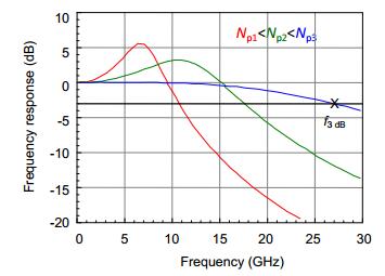
    Fig. 1. Schematic plot of intrinsic modulation response with increasing photon densities.
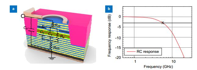
    (a) Electrical parasitic elements inside a VCSEL. (b) Low pass filter induced by the RC components.
    Fig. 2. (a) Electrical parasitic elements inside a VCSEL. (b) Low pass filter induced by the RC components.
    Simulated frequency responses of the 850-nm VCSEL with (a) single- and (b) double-confined oxide layers.
    Fig. 3. Simulated frequency responses of the 850-nm VCSEL with (a) single- and (b) double-confined oxide layers.
    TEM image of the VCSEL with double-confined oxide layers.
    Fig. 4. TEM image of the VCSEL with double-confined oxide layers.
    Optical spectra of the VSCELs with (a) 6-μm and (b) 10-μm oxide confined apertures.
    Fig. 5. Optical spectra of the VSCELs with (a) 6-μm and (b) 10-μm oxide confined apertures.
    Near field lateral modal distributions of the VSCELs with (a) 6-μm and (b) 10-μm oxide confined apertures under different bias current conditions and (c) Cross-sectional SEM image of the VCSEL.
    Fig. 6. Near field lateral modal distributions of the VSCELs with (a) 6-μm and (b) 10-μm oxide confined apertures under different bias current conditions and (c) Cross-sectional SEM image of the VCSEL.
    Frequency responses of the VSCELs with (a) 6-μm and (b) 10-μm oxide confined apertures under different bias current conditions.
    Fig. 7. Frequency responses of the VSCELs with (a) 6-μm and (b) 10-μm oxide confined apertures under different bias current conditions.
    Optical spectra and frequency responses of the differenttype VCSELs.
    Fig. 8. Optical spectra and frequency responses of the differenttype VCSELs.
    BERs of the SM VCSEL chip carried and data waveform pre-emphasized PAM-4 data at different bandwidths after BtB, 100-m, 200-m, and 300-m OM4 MMF transmissions with the corresponding eye-diagram.
    Fig. 9. BERs of the SM VCSEL chip carried and data waveform pre-emphasized PAM-4 data at different bandwidths after BtB, 100-m, 200-m, and 300-m OM4 MMF transmissions with the corresponding eye-diagram.
    BER of the 100-m OM4-MM fiber transmitted 16-QAMOFDM data for SM VCSEL under the different receiving powers.
    Fig. 10. BER of the 100-m OM4-MM fiber transmitted 16-QAMOFDM data for SM VCSEL under the different receiving powers.
    (a) Subcarrier BER responses of the 16-QAM OFDM data before and after 100-m MMF transmissions. (b) BER responses of the FM VCSEL carried 16-QAM OFDM data with and without pre-leveling under 100-m MMF transmissions under different receiving powers.
    Fig. 11. (a) Subcarrier BER responses of the 16-QAM OFDM data before and after 100-m MMF transmissions. (b) BER responses of the FM VCSEL carried 16-QAM OFDM data with and without pre-leveling under 100-m MMF transmissions under different receiving powers.
    (a) Far-filed pattern with 6 μm aperture. (b) Intensity distribution under 1 A pulse of 2-D arrays.
    Fig. 12. (a) Far-filed pattern with 6 μm aperture. (b) Intensity distribution under 1 A pulse of 2-D arrays.
    Chih-Hsien Cheng, Chih-Chiang Shen, Hsuan-Yun Kao, Dan-Hua Hsieh, Huai-Yung Wang, Yen-Wei Yeh, Yun-Ting Lu, Sung-Wen Huang Chen, Cheng-Ting Tsai, Yu-Chieh Chi, Tsung Sheng Kao, Chao-Hsin Wu, Hao-Chung Kuo, Po-Tsung Lee, Gong-Ru Lin. 850/940-nm VCSEL for optical communication and 3D sensing[J]. Opto-Electronic Advances, 2018, 1(3): 180005
    Download Citation