
Chih-Hsien Cheng, Chih-Chiang Shen, Hsuan-Yun Kao, Dan-Hua Hsieh, Huai-Yung Wang, Yen-Wei Yeh, Yun-Ting Lu, Sung-Wen Huang Chen, Cheng-Ting Tsai, Yu-Chieh Chi, Tsung Sheng Kao, Chao-Hsin Wu, Hao-Chung Kuo, Po-Tsung Lee, Gong-Ru Lin. 850/940-nm VCSEL for optical communication and 3D sensing[J]. Opto-Electronic Advances, 2018, 1(3): 180005
- Opto-Electronic Advances
- Vol. 1, Issue 3, 180005 (2018)
Abstract
Keywords
Background
To meet the demand on the rapid development of the internet at present, versatile laser diodes based optical fiber transmission has been widely applied not only in long-haul backbone (with single-mode fiber, SMF and distributed feedback laser diode, DFBLD) and medium-range metropolitan area networks (with SMF/DFBLD or single-mode vertical cavity surface emitting laser, VCSEL), but also in short-distance area networks or intra/inter data center links (with SMF/DFBLD or multi-mode fiber and multi-mode VCSEL). In recent years, the convergence and streaming with combinations of the broadband voice and video data urge the internet related industry to develop the advanced optical communication solutions which fulfill the huge global market need. All developed and developing countries have established the high-speed optical fiber network infrastructures to achieve both the fiber to the home (FTTH), cloud/mobile data storage and streaming, and the intra/inter data center applications, etc., which is an interdisciplinary integration and construction between wired and wireless communication services. Particularly, owing to the urgent requirement on the higher data transmission rate for the faster up-/down-stream data exchange in intra data centers, the currently available transmission link based on multi-mode VCSEL and multi-mode fiber at 10 Gbps/ channel has gradually found its bottleneck to supply the tremendous network flux instantaneously. Beyond the specification of the 40/100 Gbps data center that has been commercially available, the definition and design of next-generation 400-Gbps or even 1.6-Tbps transceiver module based on high-speed VCSELs at 850 nm has also been initiated toward practical applications no later than 2020.
To catch up the developing pace of huge-amount data streaming in data center for the fusion among wireless mobile, wired telecom, cloud data center, and the FTTH networks in the near future, the investigation on the VCSEL based optical transceiver circuit module with optimized transmission data rate and extended propagation distance in multi-mode fiber become important key technologies. Especially for the required transmission capacity of the cloud transmission within intra- or among inter-data-center networks, more than millions of VCSEL-multi-mode fiber (MMF) links for cloud computing located within super data centers with the least space beyond 100, 000 ft2 and the consumed power above 10 MW, which inevitably lengthens the distance between the server rooms and even among the different severs in the sever room to make the transmission line more complicated. Therefore, each VCSEL based transceiver module has to enhance its transmission rate to 100~400 Gbps to improve the total data transmission capacity in a distance as short as 50~100 m such that the module size, energy consumption and maintaining cost can be concurrently scaled down. Moreover, the fourth-generation intelligent mobile communications (4G) with the wireless transmission rate from 5 to 208 Mbps can transmit the telephone, e-mail and video and other multimedia information. For the fifth-generation intelligent mobile communications (5G), the wireless transmission rate may be achieved to 10 Gbps, which is 100 times larger than that of 4G communication. Therefore, the large capacity and fast transceiver rate of 400 Gbps optical communication provides a key technology to apply to Internet of Things (IoT), mobile networking, super high definition video, and big data. To achieve the requirement of the high-speed and large-capacity to apply to the super computers, cloud computing, and data centers, the VCSEL is developed to become the light source of the short-reach optical links because this laser has some advantages including the low power-consumption, the effectively coupling to fiber, the low threshold current, and the high power conversion efficiency.
Design of the high-speed 850-nm VCSEL
To achieve the high-speed VCSELs, the carriers and photons directly influence the modulation speed of the VCSEL for data transmission. In principle, the relaxation frequency is the natural oscillation frequency between carriers and photons in the VCSEL which can be expressed as below:
where
![]()
Figure 1.Schematic plot of intrinsic modulation response with increasing photon densities.
In addition, the second limitation on the modulation bandwidth of the VCSEL is originated from the parasitic resistance and capacitance.
![]()
Figure 2.(
To decrease the parasitic capacitance, the multiple oxide layer was proposed to replace the single oxide layer because the device capacitance is inversely proportional to the oxide layer thickness
![]()
Figure 3.Simulated frequency responses of the 850-nm VCSEL with (a) single- and (b) double-confined oxide layers.
![]()
Figure 4.TEM image of the VCSEL with double-confined oxide layers.
The third limitation to restrict the modulation bandwidth of the 850-nm VCSEL is dominated by the internal heating induced thermal effect in the active layer of the device. Without considering the damping and electrical parasitic effects, the thermal effect induced maximal modulation bandwidth can be estimated as below
where
Mode control of the high-speed 850-nm VCSEL
In the recent researches, the 850-nm multi-mode (MM) VCSELs combining with the MM fiber (MMF) to form the transmission link is one of the cost-effective solutions
The reduction on the transverse modes of the MM VCSELs to improve the data transmission becomes an important issue
![]()
Figure 5.Optical spectra of the VSCELs with (a) 6-μm and (b) 10-μm oxide confined apertures.
In addition, the lateral modal distribution for VCSEL with different sizes of the oxide-confined aperture under various bias currents is shown in
![]()
Figure 6.Near field lateral modal distributions of the VSCELs with (a) 6-μm and (b) 10-μm oxide confined apertures under different bias current conditions and (c) Cross-sectional SEM image of the VCSEL.
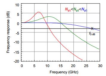
In addition, the small-size oxide-confined aperture increases the current density, which contributes to the improvement of the 3-dB modulation bandwidth (
![]()
Figure 7.Frequency responses of the VSCELs with (a) 6-μm and (b) 10-μm oxide confined apertures under different bias current conditions.
However, the oxide confinement method increases the differential resistance of the device, which needs the same current injection carriers under the higher bias, which also induces the impendence mismatch to degrade the data transmission
![]()
Figure 8.Optical spectra and frequency responses of the differenttype VCSELs.
In principle, the future research directions to improve the bandwidth of the VCSEL will include the adjustment on RC time constant of the VCSEL by decreasing either its capacitance or resistance. One straightforward way is to decrease the mesa area of the VCSEL, which can effectively reduce the device capacitance. However, this method would concurrently increase the device resistance. Therefore, the increasing doping density is expected to solve the increment on device resistance caused by reducing mesa area. The enhancement of device bandwidth is expectable with aforementioned processes. In addition, another potential approach relies on improving the epitaxial quality during growth, which effectively reduces the defects in the VCSEL so as to decrease the device resistance.
Data transmission performance of the high-speed VCSEL
For practical applications, several studies of the VCSEL for intra-data center links have been reported. In 2013, Westbergh et al. used the VCSEL with the 7-μm oxide-confined aperture to achieve the maximal modulation depth to 27 GHz, which performs the NRZ-OOK data transmission at 44 Gbps over 50-m OM4 fiber and at 47 Gbps under BtB condition
For the NRZ-OOK data transmission, the data rate is mostly dependent on the modulation bandwidth of the VCSEL because of the lower spectral usage efficiency for the NRZ-OOK data transmission. To solve this problem, the versatile data formats have been developed. The 4-level pulse amplitude modulation (PAM-4) data format is one of solutions to approach for decoding the VCSEL because the half of modulation bandwidth for the PAM-4 data format is used to achieve the same data rate as compared to the NRZ-OOK data format
Moreover, a pre-emphasis filter technology for the PAM-4 data format was proposed to apply to VCSEL, which further improves the data rate to 100 Gbps over 100-m MM fiber
![]()
Figure 9.BERs of the SM VCSEL chip carried and data waveform pre-emphasized PAM-4 data at different bandwidths after BtB, 100-m, 200-m, and 300-m OM4 MMF transmissions with the corresponding eye-diagram.
To further utilize the bandwidth of laser, the quadrature amplitude modulation orthogonal frequency division multiplexing (QAM-OFDM) was proposed to solve this problem
Moreover, Kao et al. observed the VCSEL with different transverse modes to process the 16-QAM-OFDM data format over 100-m OM4 fiber transmission
![]()
Figure 10.BER of the 100-m OM4-MM fiber transmitted 16-QAMOFDM data for SM VCSEL under the different receiving powers.
Later, the same group utilized the power of the low-frequency OFDM subcarrier to compensate the power of the high-frequency OFDM subcarriers by the pre-leveling technology, which improves the transmission performance of the 100-m OM4 fiber transmitted 16-QAM-OFDM data for the FM VCSEL with the modulation bandwidth of 22 GHz
![]()
Figure 11.(
Other applications
With the great advanced development of information technology in future high-speed internet, the applications and related markets, such as the 5G mobile networks and cloud implementation using smart service systems have become increasingly widespread. Attributed to the expansion of intelligent applications, smart cities/homes can be viewed as a complex, intelligent system that allows all kinds of electronic devices with intelligent monitoring and information transmission capabilities to interact with each other through communication technologies. To build a smart city, the sensing client is one of the most important links in the intelligent service system. For example, the major motor vehicle manufacturers deploy sensors, such as light detection and ranging (LiDAR) and depth-sensing lenses to achieve the goal of fully autonomous vehicles. LiDAR is an optical telemetry technology. When the optical radar irradiates a laser beam on the target, the distance between the target and the optical radar is measured according to the time of flight of light transmitted and received, and the position information of the target is estimated from the emission and reception angles of the laser light. To date, the direction of laser beam for a sensing system has principally been governed by an external mechanical system that incorporates macroscopic-size optical components including double-swing mirror, galvanometer-driven mirrors and polygon reflecting prism. The traditional sensor-mechanical LiDAR has many disadvantages, e.g., large size, expensive, heavy, high power consumption, low performance, low reliability, and slow scanning speed. The field of view (FOV) of LiDAR is related to beam divergence, the primary beam angle should be in range of 0.1 to 1 milliradian, and small FOV can be used for detailed local mapping, edge detection, and detailed vegetation canopy studies. Large FOV can be used for more complete ground sampling and more interactions with multiple vertical structures.
To achieve the near-infrared laser with the capability of an optical radar component, the laser device must be able to flexibly regulate the emission angle that allows active beam steering. Prof. F. Koyama's group from Tokyo Institute of Technology proposed that the laser beam steering can be successfully achieved by using GaAs-based VCSELs combined with a slow-light Bragg reflector waveguide
In 2013, Prof. F. Koyama proposed a high-resolution beam-steering device based on a vertical-cavity surface-emitting laser with a 1-mm-long active-type Bragg reflector waveguide
In addition, an optical phased array (OPA) with multiple optical antenna elements may provide equal-intensity coherent signals by modulating the phase of individual antenna. In 2013, J. Sun et al., at Massachusetts Institute of Technology (MIT) demonstrated a large-scale nanophotonic phased array to achieve beam steering built on a silicon photonic platform
![]()
Figure 12.(
In 2015, J. C. Hulme, et al. from University of California, Santa Barbara presented the first fully-integrated two-dimensional beam-steering chip on the photonic integrated circuit (PIC) platform
Conclusions
With the development of VCSEL and application requirements, VCSEL not only played an important role of the high-speed and large-capacity to be applied to the supercomputers, cloud computing, 5G communications, and data centers, also applied to face recognition, light detection and ranging (LiDAR) and VR (virtual reality)/AR (augmented reality)/MR (mixed reality) and so on. Through the increasing diversification of market demand for VCSEL, commercial technology companies and research institutions are following the trend of in-depth research, optimizing VCSEL performance and improving output power. Believed that in the near future, VCSEL will have a better development.
Acknowledgements
The authors would like to thank Prof. K Iga and Prof. F Koyama of Tokyo Institute of Technology, Prof. N. Holonyak Jr. and Prof. M. Feng of UIUC, Prof. C. Chang-Hasnain of UC Berkeley, and Prof. S. C. Wang and Prof. T. C. Lu of Chiao Tung University for their insightful suggestions and discussions during the development of GaAs-based VCSEL technology, Crosslight for providing simulation modeling calculate technical support, and Picosun for providing atomic layer deposition technical support. This work was supported by the Ministry of Science and Technology, Taiwan, China (Grants No. MOST 104-2221-E-002-117-MY3, MOST 106-2221- E-002-152-MY3 and MOST 106-2218-E-005-001-) and Excellent Research Projects of Taiwan University (Grant No. NTU-ERP-105R89081).
Competing interests
The authors declare no competing financial interests.
References
[1] P Westbergh, J S Gustavsson, Å Haglund, M Skold, A Joel et al. High-speed, low-current-density 850 nm VCSELs. IEEE J Sel Top Quantum Electron, 15, 694-703(2009).
[2] S B Healy, E P O'Reilly, J S Gustavsson, P Westbergh, Å Haglund et al. Active region design for high-speed 850-nm VCSELs. IEEE J Quantum Electron, 46, 506-512(2010).
[3] K L Lear, A Mar, K D Choquette, S P Kilcoyne, Jr R P Schneider et al. High-frequency modulation of oxide-confined vertical cavity surface emitting lasers. Electron Lett, 32, 457-458(1996).
[4] LearK LHietalaV MHouH QBanasJHammonsB EHigh-speed 850 nm oxide-confined vertical cavity surface emitting lasers. In Nuss M, Bowers J. Ultrafast Electronicsand Optoelectronics (Optical Society of America, Washington, DC, 1997).Lear K L, Hietala V M, Hou H Q, Banas J, Hammons B E et al. High-speed 850 nm oxide-confined vertical cavity surface emitting lasers. In Nuss M, Bowers J. Ultrafast Electronics and Optoelectronics (Optical Society of America, Washington, DC, 1997).
[5] Y H Chang, H C Kuo, F I Lai, K F Tzeng, H C Yu et al. High speed (> 13 GHz) modulation of 850 nm vertical cavity surface emitting lasers (VCSELs) with tapered oxide confined layer. IEE Proc-Optoelectron, 152, 170-173(2005).
[6] Y Ou, J S Gustavsson, P Westbergh, A Haglund, A Larsson et al. Impedance characteristics and parasitic speed limitations of high-speed 850-nm VCSELs. IEEE Photon Technol Lett, 21, 1840-1842(2009).
[9] J W Shi, Z R Wei, K L Chi, J W Jiang, J M Wun et al. Single-mode, high-speed, and high-power vertical-cavity surface-emitting lasers at 850 nm for short to medium reach (2 km) optical interconnects. J Lightwave Technol, 31, 4037-4044(2013).
[10] MutigAPhysical processes in lasers and VCSEL design. In High Speed VCSELs for Optical Interconnects (Springer, Berlin, Heidelberg, 2011: 19-84)Mutig A. Physical processes in lasers and VCSEL design. In High Speed VCSELs for Optical Interconnects (Springer, Berlin, Heidelberg, 2011: 19-84).
[11] A N Al-Omari, K L Lear. VCSELs with a self-aligned contact and copper-plated heatsink. IEEE Photon Technol Lett, 17, 1767-1769(2005).
[12] A Larsson, P Westbergh, J Gustavsson, Å Haglund. High-speed low-current-density 850 nm VCSELs. Proc SPIE, 7615, 761505(2010).
[13] A Gholami, D Molin, P Sillard. Compensation of chromatic dispersion by modal dispersion in MMF- and VCSEL-based gigabit Ethernet transmissions. IEEE Photon Technol Lett, 21, 645-647(2009).
[14] S A Blokhin, J A Lott, A Mutig, G Fiol, N N Ledentsov et al. Oxide-confined 850 nm VCSELs operating at bit rates up to 40 Gbit/s. Electron Lett, 45, 501-503(2009).
[15] P Westbergh, J S Gustavsson, B Kögel, A Haglund, A Larsson et al. 40 Gbit/s error-free operation of oxide-confined 850 nm VCSEL. Electron Lett, 46, 1014-1016(2010).
[16] K Szczerba, P Westbergh, J Karout, J S Gustavsson, Å Haglund et al. 4-PAM for high-speed short-range optical communications. IEEE J Opt Commun Netw, 4, 885-894(2012).
[17] K D Choquette, K M Geib, R D Briggs, A A Allerman, J J Hindi. Single transverse mode selectively oxidized vertical-cavity lasers. Proc SPIE, 3946, 230-233(2000).
[18] Å Haglund, J S Gustavsson, J Vukŭsić, P Modh, A Larsson. Single fundamental-mode output power exceeding 6 mW from VCSELs with a shallow surface relief. IEEE Photon Technol Lett, 16, 368-370(2004).
[19] A Furukawa, M Hoshi, S Sasaki, A Matsuzono, K Moritoh et al. High-power single-transverse-mode holey VCSELs (Invited Paper). Proc SPIE, 5722, 183-190(2005).
[20] R Safaisini, K Szczerba, P Westbergh, E Haglund, B Kögel et al. High-speed 850 nm Quasi-single-mode VCSELs for extended-reach optical interconnects. IEEE J Opt Commun Netw, 5, 686-695(2013).
[21] R Michalzik, K J Ebeling. Generalized BV diagrams for higher order transverse modes in planar vertical-cavity laser diodes. IEEE J Quantum Electron, 31, 1371-1379(1995).
[22] J S Gustavsson, A Haglund, J Bengtsson, P Modh, A Larsson. Dynamic behavior of fundamental-mode stabilized VCSELs using a shallow surface relief. IEEE J Quantum Electron, 40, 607-619(2004).
[23] Y Liu, W C Ng, B Klein, K Hess. Effects of the spatial nonuniformity of optical transverse modes on the modulation response of vertical-cavity surface-emitting lasers. IEEE J Quantum Electron, 39, 99-108(2003).
[24] D Vakhshoori, J D Wynn, G J Zydzik, R E Leibenguth, M T Asom et al. Top-surface emitting lasers with 1.9 V threshold voltage and the effect of spatial hole burning on their transverse mode operation and efficiencies. Appl Phys Lett, 62, 1448-1450(1993).
[25] M H MacDougal, J Geske, C K Lin, A E Bond, P D Dapkus. Low resistance intracavity-contacted oxide-aperture VCSELs. IEEE Photon Technol Lett, 10, 9-11(1998).
[26] I Harrison, H P Ho, B Tuck, M Henini, O H Hughes. Zn diffusion-induced disorder in AlAs/GaAs superlattices. Semicond Sci Technol, 4, 841-846(1989).
[27] Y J Yang, T G Dziura, T Bardin, S C Wang, R Fernandez. Continuous wave single transverse mode vertical-cavity surface-emitting lasers fabricated by helium implantation and zinc diffusion. Electron Lett, 28, 274-276(1992).
[28] J W Shi, C C Chen, Y S Wu, S H Guol, C Kuo et al. High-power and high-speed Zn-diffusion single fundamental-mode vertical-cavity surface-emitting lasers at 850-nm wavelength. IEEE Photon Technol Lett, 20, 1121-1123(2008).
[29] H Y Kao, Y C Chi, C Y Peng, S F Leong, C K Chang et al. Modal linewidth dependent transmission performance of 850-nm VCSELs with encoding PAM-4 over 100-m MMF. IEEE J Quantum Electron, 53, 8000408(2017).
[30] P Westbergh, R Safaisini, E Haglund, B Kögel, J S Gustavsson et al. High-speed 850 nm VCSELs with 28 GHz modulation bandwidth operating error-free up to 44 Gbit/s. Elect Lett, 48, 1145-1147(2012).
[31] P Westbergh, R Safaisini, E Haglund, J S Gustavsson, A Larsson et al. High-speed oxide confined 850-nm VCSELs operating error-free at 40 Gb/s up to 85oC. IEEE Photon Technol Lett, 25, 768-771(2013).
[32] K L Chi, Y X Shi, X N Chen, J Chen, Y J Yang et al. Single-mode 850-nm VCSELs for 54-Gb/s ON-OFF keying transmission over 1-km multi-mode fiber. IEEE Photon Technol Lett, 28, 1367-1370(2016).
[33] K Szczerba, P Westbergh, E Agrell, M Karlsson, P A Andrekson et al. Comparison of intersymbol interference power penalties for OOK and 4-PAM in short-range optical links. J Lightwave Technol, 31, 3525-3534(2013).
[36] K Szczerba, P Westbergh, M Karlsson, P A Andrekson, A Larsson. 60 Gbits error-free 4-PAM operation with 850 nm VCSEL. Elect Lett, 49, 953-955(2015).
[39] LavrencikJVarugheseSThomasV ALandryGSunY100Gbps PAM-4 transmission over 100m OM4 and wideband fiber using 850nm VCSELs. In 42nd European Conference on Optical Communication 1-3 (IEEE, 2016)Lavrencik J, Varughese S, Thomas V A, Landry G, Sun Y et al. 100Gbps PAM-4 transmission over 100m OM4 and wideband fiber using 850nm VCSELs. In 42nd European Conference on Optical Communication 1-3 (IEEE, 2016).
[40] KaoH YTsaiC TLeongS FPengC YChiY C Single-mode VCSEL for pre-emphasis PAM-4 transmission up to 64 Gbit/s over 100-300 m in OM4 MMF. Photon Res. Accepted 17 Dec 2017. Doc. ID: 312994.Kao H Y, Tsai C T, Leong S F, Peng C Y, Chi Y C et al. Single-mode VCSEL for pre-emphasis PAM-4 transmission up to 64 Gbit/s over 100-300 m in OM4 MMF. Photon Res. Accepted 17 Dec 2017. Doc. ID: 312994.
[41] F Karinou, L Deng, R R Lopez, K Prince, J B Jensen et al. Performance comparison of 850-nm and 1550-nm VCSELs exploiting OOK, OFDM, and 4-PAM over SMF/MMF links for low-cost optical interconnects. Opt Fiber Technol, 19, 206-212(2013).
[42] Y C Chi, Y C Li, H Y Wang, P C Peng, H H Lu et al. Optical 16-QAM-52-OFDM transmission at 4 Gbit/s by directly modulating a coherently injection-locked colorless laser diode. Opt Express, 20, 20071-20077(2012).
[43] C Y Lin, Y C Chi, C T Tsai, H Y Wang, G R Lin. 39-GHz millimeter-wave carrier generation in dual-mode colorless laser diode for OFDM-MMWoF transmission. IEEE J Sel Top Quantum Electron, 21, 1801810(2015).
[44] S C J Lee, S Randel, F Breyer, A M J Koonen. PAM-DMT for intensity-modulated and direct-detection optical communication systems. IEEE Photon Technol Lett, 21, 1749-1751(2009).
[45] D J F Barros, S K Wilson, J M Kahn. Comparison of orthogonal frequency-division multiplexing and pulse-amplitude modulation in indoor optical wireless links. IEEE Trans Commun, 60, 153-162(2012).
[46] I C Lu, C C Wei, H Y Chen, K Z Chen, C H Huang et al. Very high bit-rate distance product using high-power single-mode 850-nm VCSEL with discrete multitone modulation formats through OM4 multimode fiber. IEEE J Sel Top Quantum Electron, 21, 1701009(2015).
[48] C T Tsai, C Y Peng, C Y Wu, S F Leong, H Y Kao et al. Multi-mode VCSEL chip with high-indium-density InGaAs/AlGaAs quantum-well pairs for QAM-OFDM in multi-mode fiber. IEEE J Quantum Electron, 53, 2400608(2017).
[49] KaoH YTsaiC TLeongS FPengC YChiY C Comparison of single-/few-/multi-mode 850 nm VCSELs for optical OFDM transmission. Opt Express25, 16347-16363 (2017)Kao H Y, Tsai C T, Leong S F, Peng C Y, Chi Y C et al. Comparison of single-/few-/multi-mode 850 nm VCSELs for optical OFDM transmission. Opt Express 25, 16347-16363 (2017).
[50] H Y Kao, Y C Chi, C T Tsai, S F Leong, C Y Peng et al. Few-mode VCSEL chip for 100-Gb/s transmission over 100 m multimode fiber. Photon Res, 5, 507-515(2017).
[51] X D Gu, T Shimada, A Fuchida, A Matsutani, A Imamura et al. Beam steering in GaInAs/GaAs slow-light Bragg reflector waveguide amplifier. Appl Phys Lett, 99, 211107(2011).
[52] F Koyama, X D Gu. Beam steering, beam shaping, and intensity modulation based on VCSEL photonics. IEEE J Sel Top Quantum Electron, 19, 1701510(2013).
[53] J Sun, E Timurdogan, A Yaacobi, E S Hosseini, M R Watts. Large-scale nanophotonic phased array. Nature, 493, 195-199(2013).
[54] C T DeRose, R D Kekatpure, D C Trotter, A Starbuck, J R Wendt et al. Electronically controlled optical beam-steering by an active phased array of metallic nanoantennas. Opt Express, 21, 5198-5208(2013).
[55] J C Hulme, J K Doylend, M J R Heck, J D Peters, M L Davenport et al. Fully integrated hybrid silicon two dimensional beam scanner. Opt Express, 23, 5861-5874(2015).


Set citation alerts for the article
Please enter your email address

© Copyright 2018-2021 | Chinese Laser Press. All Rights Reserved 沪ICP备15018463号-20