• Journal of Semiconductors
  • Vol. 41, Issue 6, 062302 (2020)
H. J. Lee1、2, S. Y. Ko1, Y. H. Kim1, and J. Nah2
Author Affiliations
  • 1i3system, Inc., 26-32, Gajeongbuk-ro, Daejeon, 34113, Yuseong-gu, Korea
  • 2Department of Electrical Engineering, Chungnam National University, Daejeon, 34134, Yuseong-gu, Korea
  • show less
    DOI: 10.1088/1674-4926/41/6/062302 Cite this Article
    H. J. Lee, S. Y. Ko, Y. H. Kim, J. Nah. Strain-induced the dark current characteristics in InAs/GaSb type-II superlattice for mid-wave detector[J]. Journal of Semiconductors, 2020, 41(6): 062302 Copy Citation Text show less
    (Color online) (a) The schematic of the InAs/GaSb T2SL MWIR epi. structure with nBn structure. (b) TEM image of the absorber layer with InAs/GaSb 10/10 MLs. The inset on right corner shows a magnitude view taken in HAADF mode. (c) The schematics of the InAs/GaSb T2SL nBn device fabrication process. Fist, each pixel is isolated by etching the top contact layer and the barrier using C6H8O7/H3PO4/H2O2/H2O solution. After wet-treatment to remove a native oxide at the surface, SiO2 passivation layer is deposited using PECVD. Finally, the contact metal is evaporated for both pixels and common electrode.
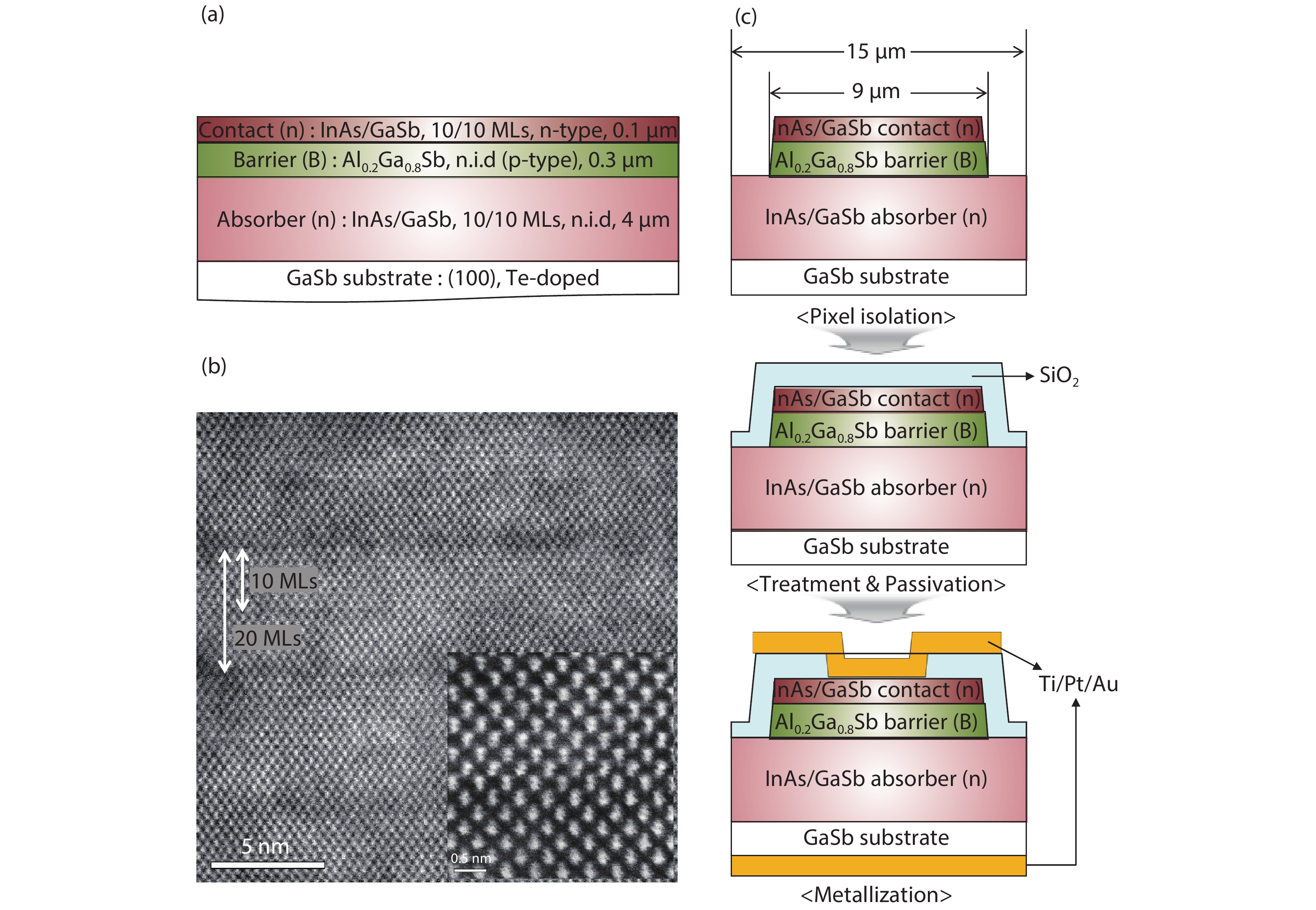
    Fig. 1. (Color online) (a) The schematic of the InAs/GaSb T2SL MWIR epi. structure with nBn structure. (b) TEM image of the absorber layer with InAs/GaSb 10/10 MLs. The inset on right corner shows a magnitude view taken in HAADF mode. (c) The schematics of the InAs/GaSb T2SL nBn device fabrication process. Fist, each pixel is isolated by etching the top contact layer and the barrier using C6H8O7/H3PO4/H2O2/H2O solution. After wet-treatment to remove a native oxide at the surface, SiO2 passivation layer is deposited using PECVD. Finally, the contact metal is evaporated for both pixels and common electrode.
    (Color online) (a) The dark current density versus applied bias at 80 K. The identical fabrication process is used for device fabrication on the wafers A and B. Approximately, one order of magnitude higher dark current density is observed from the devices on the wafer A. (b) Arrhenius plots of the devices fabricated on the wafers A and B. Both devices demonstrate diffusion-limited current but different activation energies. The plot indicates that the minority carrier lifetime in the absorber layer of the devices on the wafer B is longer than those on the wafer A.
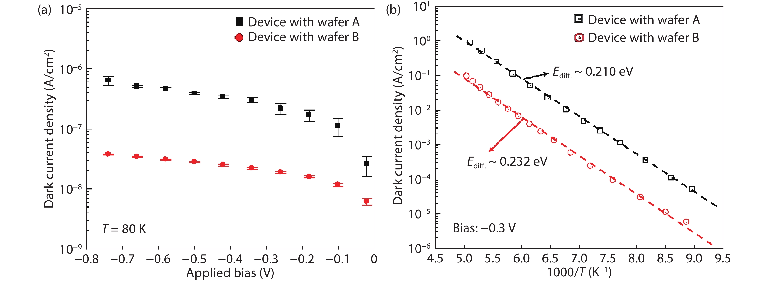
    Fig. 2. (Color online) (a) The dark current density versus applied bias at 80 K. The identical fabrication process is used for device fabrication on the wafers A and B. Approximately, one order of magnitude higher dark current density is observed from the devices on the wafer A. (b) Arrhenius plots of the devices fabricated on the wafers A and B. Both devices demonstrate diffusion-limited current but different activation energies. The plot indicates that the minority carrier lifetime in the absorber layer of the devices on the wafer B is longer than those on the wafer A.
    (Color online) Spectral response of the devices fabricated on the wafers A and B. The cut-off wavelength of the devices on the wafer B is shorter than those on the wafer A. The result is consistent with the results in Fig. 2, exhibiting difference activation energies.
    Fig. 3. (Color online) Spectral response of the devices fabricated on the wafers A and B. The cut-off wavelength of the devices on the wafer B is shorter than those on the wafer A. The result is consistent with the results in Fig. 2, exhibiting difference activation energies.
    High-resolution X-ray omega-2theta scan data of InAs/GaSb T2SL and Al0.2Ga0.8Sb around GaSb (004) peak.
    Fig. 4. High-resolution X-ray omega-2theta scan data of InAs/GaSb T2SL and Al0.2Ga0.8Sb around GaSb (004) peak.
    No. waferStrain typePeriodicity (Å)Mismatch (ppm)
    ATensile59.18788.6
    BTensile59.0667.37
    Table 1. Analysis of HRXRD patterns.
    H. J. Lee, S. Y. Ko, Y. H. Kim, J. Nah. Strain-induced the dark current characteristics in InAs/GaSb type-II superlattice for mid-wave detector[J]. Journal of Semiconductors, 2020, 41(6): 062302
    Download Citation