
H. J. Lee, S. Y. Ko, Y. H. Kim, J. Nah. Strain-induced the dark current characteristics in InAs/GaSb type-II superlattice for mid-wave detector[J]. Journal of Semiconductors, 2020, 41(6): 062302
- Journal of Semiconductors
- Vol. 41, Issue 6, 062302 (2020)
Abstract
1. Introduction
There is an increasing demand for infrared detectors in a wide variety of applications, such as surveillance equipment, medical devices, and military applications. To date, InSb and HgCdTe (MCT) have been the main block for conventional infrared detectors because they demonstrate relatively high quantum efficiency and low dark current[
One of the crucial factors determining the performance of T2SL detector is the growth quality of the epitaxial (epi.) layer, which is closely related to balanced strain[
In this work, we report that the interfacial properties of InAs/GaSb T2SL layer can be largely varied even if the epi. wafers are prepared by the same MBE protocol, significantly affecting the dark current characteristics of the devices. By analyzing temperature-dependent dark current characteristics and spectral responses of the T2SL layer, the properties of the interfacial layer have been investigated. Further, the strain of InAs/GaSb T2SL layer was also verified by analyzing the mismatch using the HRXRD patterns. Our study indicates that the minority carrier lifetime significantly increased as the tensile strain on the InAs/GaSb T2SL is more compensated by compressive strain originated from the 'InSb-like' interface, reducing the dark current density of the devices. Consequently, the dark current density of the fabricated devices on the strain compensated InAs/GaSb T2SL layer demonstrates the dark current density less than 2 × 10⁻⁵ A/cm2 at 120 K.
2. Experiments
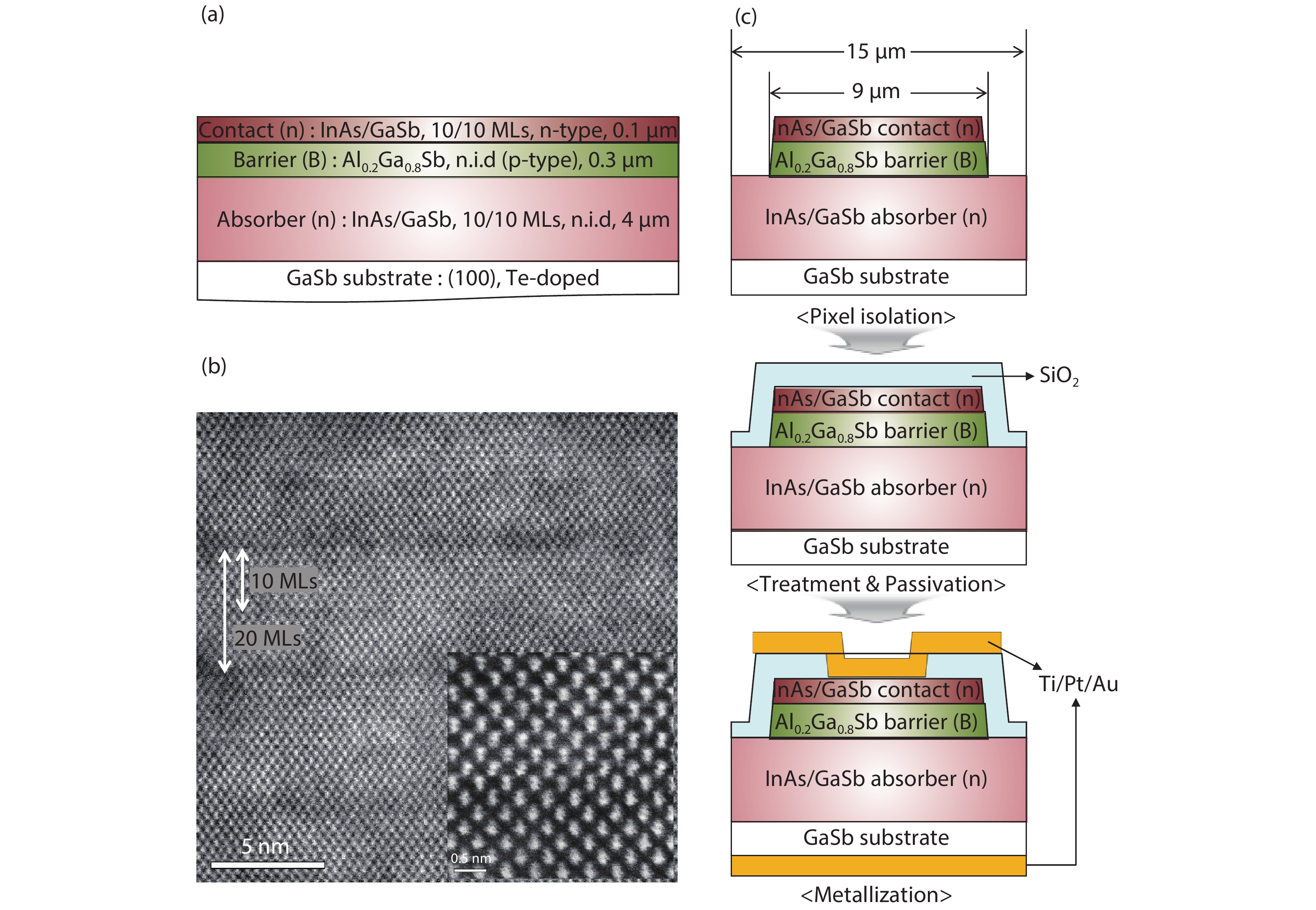
The crystal structure of the InAs/GaSb T2SL mid-wave infrared (MWIR) studied in this work is shown in Fig. 1(a). The absorber layer consists of InAs/GaSb 10/10 MLs, which has a bandgap energy of 0.244 eV, calculated using empirical pseudopotential method (EPM) at 77 K. The absorber layer in Fig. 1(b) clearly shows the periodic crystal structure, where the inset shows dumbbell-like structures of InAs and GaSb. To compose nBn structure that can effectively reduce the dark current, the barrier layer was designed with Al0.2Ga0.8Sb that has a relatively high conduction band energy barrier (~ 1 eV) with almost zero valence band offset. For experiment, two different wafers (A and B) were grown individually but with the identical design and the same MBE protocol. Using two different epi. wafers, InAs/GaSb T2SL nBn devices with a 15 μm pitch were fabricated as briefly described in Fig. 1(c). Here, each pixel is isolated in 9 × 9 cm2 area by etching the top contact layer and the barrier layer using C6H8O7 : H3PO4 : H2O2 : H2O (15 : 20 : 12 : 40) solution for 25 s, followed by immersing in HCl : H2O (1 : 10) solution for 60 s to remove a native oxide at the surface. For passivation, a 300 nm-thick SiO2 was deposited using a plasma-enhanced chemical vapor deposition (PECVD) at 250 °C for 45 s. Afterwards, Ti/Pt/Au (30/70/100 nm) layer was deposited on the contact layer of each pixel on the top side and on the GaSb substrate as a bottom common electrode for the electrical characterization.
![]()
Figure 1.(Color online) (a) The schematic of the InAs/GaSb T2SL MWIR epi. structure with nBn structure. (b) TEM image of the absorber layer with InAs/GaSb 10/10 MLs. The inset on right corner shows a magnitude view taken in HAADF mode. (c) The schematics of the InAs/GaSb T2SL nBn device fabrication process. Fist, each pixel is isolated by etching the top contact layer and the barrier using C6H8O7/H3PO4/H2O2/H2O solution. After wet-treatment to remove a native oxide at the surface, SiO2 passivation layer is deposited using PECVD. Finally, the contact metal is evaporated for both pixels and common electrode.
3. Results and discussion
Fig. 2(a) shows the dark current density of the devices fabricated on the wafers A and B which are measured at 80 K. We note that the identical fabrication process is employed for the devices on both wafers A and B. The devices on two different wafers exhibit approximately one order of magnitude difference in the dark current density even if the same device design and process are employed. The dark current at cryogenic temperature (80 K) could be originated from different parts of the device. For example, it can be either from the depletion region in the vicinity between the barrier and the absorber or from the surface region covered with the passivation film. Thus, to further investigate the devices, the dark current density was measured by increasing temperature to 200 K. As the temperature increases, the dark current density is dominated by the diffusion current and recombination current from the absorber layer, which is greatly affected by the crystal quality of absorber layer rather than the process condition.
![]()
Figure 2.(Color online) (a) The dark current density versus applied bias at 80 K. The identical fabrication process is used for device fabrication on the wafers A and B. Approximately, one order of magnitude higher dark current density is observed from the devices on the wafer A. (b) Arrhenius plots of the devices fabricated on the wafers A and B. Both devices demonstrate diffusion-limited current but different activation energies. The plot indicates that the minority carrier lifetime in the absorber layer of the devices on the wafer B is longer than those on the wafer A.
Next, temperature-dependent dark current density was measured at a bias voltage of –0.3 V for the devices on two different wafers as shown in Fig. 2(b). Both devices demonstrate the diffusion-limited dark current characteristics but with slightly different activation energies. The dark current density of the devices fabricated on the wafer B is approximately one order smaller than those on the wafer A. This result shows that the minority carrier lifetime in the absorber layer of the wafer B is longer than that of wafer A. Different minority carrier lifetime can be attributed to overall strain on the InAs/GaSb T2SL layer. Unbalanced strain can lead to the formation of extended defects that act as SRH recombination lefts[
The overall strain on the T2SL affects not only the electrical properties as described above but also the optical properties[
![]()
Figure 3.(Color online) Spectral response of the devices fabricated on the wafers A and B. The cut-off wavelength of the devices on the wafer B is shorter than those on the wafer A. The result is consistent with the results in
To further unveil the origin of different electrical and optical properties, HRXRD pattern was measured to compare the overall strain of the wafers A and B. Fig. 4 qualitatively shows the difference in the peak between GaSb substrate and the first superlattice (SL). The SL (+1) peak of the wafer B is closer to GaSb substrate than that of the wafer A. As shown in Table 1. the average lattice mismatch and periodicity obtained from HRXRD pattern quantitatively show different T2SL quality of the wafers A and B. The thickness of one period InAs/GaSb T2SL (periodicity) is calculated to be 59.18 Å for wafer A and 59.06 Å for wafer B, respectively. Although the periodicity of both wafers A and B is close to the original layer design and the growth of InAs/GaSb T2SL layer has been performed as expected; however, the mismatch values are clearly different: the mismatch of wafers A and B are 788.6 and 67.37 ppm, respectively. We believed that randomly formed 'InSb-like' interfacial layer during the MBE process greatly reduced the mismatch. The results of the HRXRD pattern in Table 1 and the dark current characteristics in Fig. 2 clearly demonstrate that overall strain on InAs/GaSb T2SL layer affects the minority carrier lifetime[
![]()
Figure 4.High-resolution X-ray omega-2theta scan data of InAs/GaSb T2SL and Al0.2Ga0.8Sb around GaSb (004) peak.
4. Conclusion
In this work, the electrical, optical and structural properties of the InAs/GaSb T2SL MWIR epi. structures were analyzed. Using dark current density measurement, FTIR and HRXRD analysis, the interfacial property of the InAs/GaSb T2SL layer has been successfully analyzed. The results demonstrate that the minority carrier lifetime can be extended by compensating the tensile strain of the InAs/GaSb T2SL layer through unintentionally formed 'InSb-like' interfacial layer during the MBE growth process. Through strain compensation of the tensile strained InAs/GaSb T2SL layer, the dark current density smaller than 2 × 10⁻⁵ A/cm2 has been achieved at 120 K. Therefore, high performance InAs/GaSb T2SL MWIR photodetectors can be fabricated reproducibly by developing the growth process to intentionally form 'InSb-like' interfacial layer.
Acknowledgements
This research was supported by the research fund of Chungnam National University and the author would like to A. Liu at IQE for helpful discussions. The authors wish also to thank his colleagues at i3system, Inc. for processing of the devices.
References
[1] A Rogalski. Recent process in infrared detector technologies. Infrared Phys Technol, 54, 136(2011).
[2] A Rogalski, P Martyniuk, M Kopytko. Challenges of small pixel infrared detectors: A review. Rep Prog Phys, 79, 1(2016).
[3] A Rogalski. Next decade in infrared detectors. Proc SPIE, 10433, 104330L(2017).
[4] D Rhiger, R Kvaas, S Harris et al. Progress with type-II superlattice IR detector arrays. Proc SPIE, 6542, 654202(2007).
[5] N Herres, F Fuchs, J Schmitz et al. Effect of interfacial bonding on the structural and vibrational properties of InAs/GaSb superlattices. Phys Rev B, 53, 15688(1996).
[6] J Steinshnider, M Weimer, R Kaspi et al. Visualizing interfacial structure at non-common-atom heterojunctions with cross-sectional scanning tunneling microscopy. Phys Rev Lett, 85, 2953(2000).
[7] S Lyapin, P Klipstein, N Mason et al. Raman selection rules for the observation of interface modes in InAs/GaSb superlattices. Phy Rev Lett, 74, 3285(1995).
[8] E Plis, S Annamalai, K Posani et al. Midwave infrared type-II InAs/GaSb superlattice detectors with mixed interfaces. J Appl Phys, 100, 014510(2006).
[9] J Rodriguez, P Christol, L Cerutti et al. MBE growth and characterization of type-II InAs/GaSb superlattices for mid-infrared detection. J Cryst Growth, 274, 6(2005).
[10] G Liu, B Fruhberger, I Schuller et al. Quantitative structural characterization of InAs/GaSb superlatties. J Appl Phys, 100, 063536(2006).
[11] D Zuo, P Qiao, D Wasserman et al. Direct observation of minority carrier lifetime improvement in InAs/GaSb type-II superlattice photodiodes via interfacial layer control. Appl Phys Lett, 102, 141107(2013).
[12] Y Zhang, W Ma, J Huang et al. Long wavelength infrared InAs/GaSb superlattice photodetectors with InSb-like and mixed interfaces. IEEE J Quantum Electron, 47, 1475(2011).
[13] Y Song, S Wang, C Asplund et al. Growth optimization, strain compensation and structure design of InAs/GaSb type-II superlattices for mid-infrared imaging. Cryst Struct Theory Appl, 02, 46(2013).
[14] H Kim, Y Meng, J Rouviére et al. Atomic resolution mapping of interfacial intermixing and segration in InAs/GaSb superlattices: A correlative study. J Appl Phys, 113, 103511(2013).
[15] K Mahalingam, H Haugan, G Brown et al. Strain analysis of compositionally tailored interfaces in InAs/GaSb superlattices. Appl Phys Lett, 103, 211605(2013).
[16] Y Ashuach, E Lakin, C Saguy et al. Atomic intermixing and interface roughness in short-period InAs/GaSb superlattices for infrared photodetectors. J Appl Phys, 116, 124315(2014).
[17] Y Meng, H Kim, J Rouviére et al. Digital model for X-ray diffraction with application to composition and strain determination in strained InAs/GaSb superlattices. J Appl Phys, 116, 013513(2014).
[18] Y Sun, G Wang, W Xiang et al. 320 × 256 high operating temperature mid-infrared focal plane arrays based on type-II InAs/GaSb superlattice. Superlattices Microstruct, 111, 783(2017).
[19] S Höglund, R Naureen, M Ivanov et al. Type II superlattices: HOT MWIR production and development at IRnova. Proc SPIE, 11002, 110020U(2019).

Set citation alerts for the article
Please enter your email address
© Copyright 2018-2021 | Chinese Laser Press. All Rights Reserved 沪ICP备15018463号-20