• Journal of Inorganic Materials
  • Vol. 34, Issue 1, 79 (2019)
Yu LIANG1、2, Ling-Yan LIANG1, Wei-Hua WU1, Yu PEI1, Zhi-Qiang YAO2, Hong-Tao CAO1, [in Chinese]1、2, [in Chinese]1, [in Chinese]1, [in Chinese]1, [in Chinese]2, and [in Chinese]1
Author Affiliations
  • 11. Key Laboratory of Graphene Technologies and Applications of Zhejiang Province, Ningbo Institute of Materials Technology and Engineering, Chinese Academy of Sciences, Ningbo 315201, China
  • 22. State Centre for International Cooperation on Designer Low-Carbon and Environmental Materials (ICDLCEM), School of Material Science and Engineering, Zhengzhou University, Zhengzhou 450001, China
  • show less
    DOI: 10.15541/jim20180167 Cite this Article
    Yu LIANG, Ling-Yan LIANG, Wei-Hua WU, Yu PEI, Zhi-Qiang YAO, Hong-Tao CAO, [in Chinese], [in Chinese], [in Chinese], [in Chinese], [in Chinese], [in Chinese]. Microfluidic-method-processed p-type NiOx Thin-film Transistors[J]. Journal of Inorganic Materials, 2019, 34(1): 79 Copy Citation Text show less
    Illustration of the preparation process of PDMS moulds
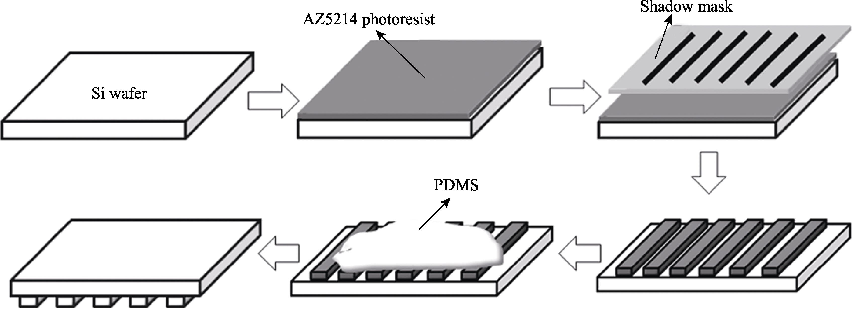
    . Illustration of the preparation process of PDMS moulds
    Illustration of the patterning process by capillary method
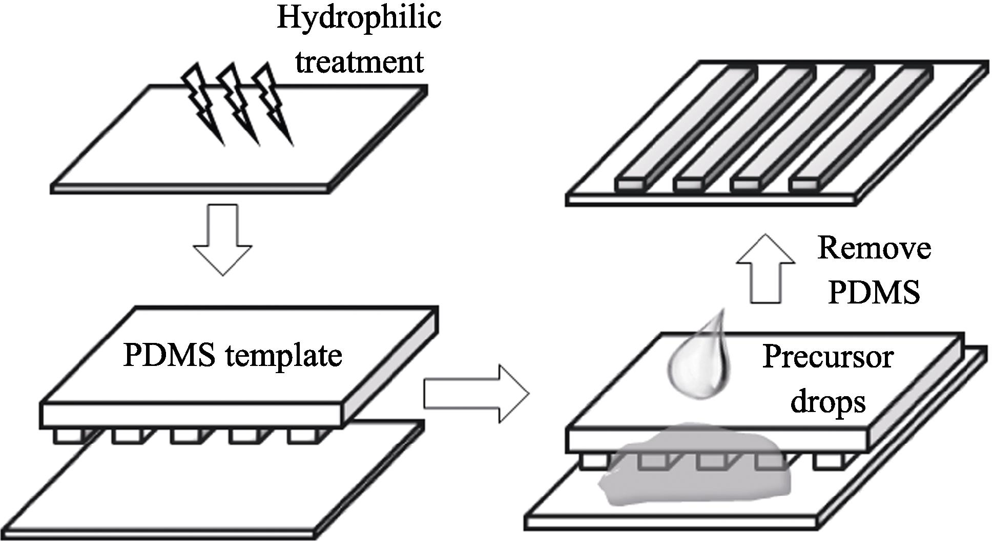
    . Illustration of the patterning process by capillary method
    Thermogravimetric and differential thermal analysis (TG-DTA) curves of NiO precursor
    . Thermogravimetric and differential thermal analysis (TG-DTA) curves of NiO precursor
    XRD patterns of NiO powders
    . XRD patterns of NiO powders
    (a) Optical microscope image of a substrate patterned with NiO stripes with inset showing a close-up view; (b) Height fluctuation across the NiO stripe margin obtained by atomic force microscopy
    . (a) Optical microscope image of a substrate patterned with NiO stripes with inset showing a close-up view; (b) Height fluctuation across the NiO stripe margin obtained by atomic force microscopy
    Schematic structure of the fabricated TFT device (a), output curves of the TFTs annealed at 300℃ (b) and 350℃ (c), and transfer curves of the corresponding TFTs (d)
    . Schematic structure of the fabricated TFT device (a), output curves of the TFTs annealed at 300℃ (b) and 350℃ (c), and transfer curves of the corresponding TFTs (d)
    Yu LIANG, Ling-Yan LIANG, Wei-Hua WU, Yu PEI, Zhi-Qiang YAO, Hong-Tao CAO, [in Chinese], [in Chinese], [in Chinese], [in Chinese], [in Chinese], [in Chinese]. Microfluidic-method-processed p-type NiOx Thin-film Transistors[J]. Journal of Inorganic Materials, 2019, 34(1): 79
    Download Citation