
Chaohui Li, Jun Deng, Weiye Sun, Leilei He, Jianjun Li, Jun Han, Yanli Shi. Improvement of tunnel compensated quantum well infrared detector[J]. Journal of Semiconductors, 2019, 40(12): 122902
- Journal of Semiconductors
- Vol. 40, Issue 12, 122902 (2019)
![Schematic diagram of the multi-quantum well infrared detector with tunnel compensation structure[14] (under the reverse bias).](/richHtml/jos/2019/40/12/122902/img_1.jpg)
Fig. 1. Schematic diagram of the multi-quantum well infrared detector with tunnel compensation structure[14 ] (under the reverse bias).
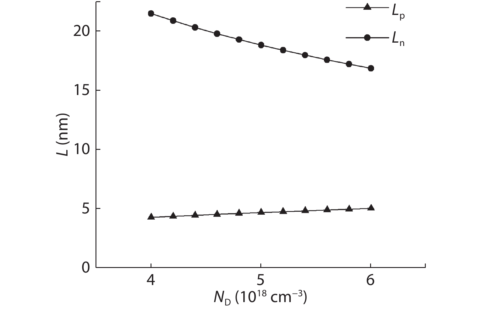
Fig. 2. The relationship between N D and depletion layer width (N A = 2 × 1019 cm–3).
Fig. 3. The relationship between L w and sub-levels. E 1 is the first level, E 2 is the second level and E b is the barrier height.
Fig. 4. Schematic diagram of the improved structure under the reverse bias.
Fig. 5. The relationship between the gain and wavelength of different numbers of wells: (a) single well, (b) double well and (c) triple well.
Fig. 6. Response spectrum of sample at 77 K.
Fig. 7. Dark current versus applied bias of sample at 77 K. (a) Forward bias. (b) Reverse bias.
Fig. 8. Blackbody response test of sample at 77 K.
| ||||||||||||||||||||||||||||||||||||||||
Table 1. Structural parameters of the experimental sample.

Set citation alerts for the article
Please enter your email address
© Copyright 2018-2021 | Chinese Laser Press. All Rights Reserved 沪ICP备15018463号-20