
Chaohui Li, Jun Deng, Weiye Sun, Leilei He, Jianjun Li, Jun Han, Yanli Shi. Improvement of tunnel compensated quantum well infrared detector[J]. Journal of Semiconductors, 2019, 40(12): 122902
- Journal of Semiconductors
- Vol. 40, Issue 12, 122902 (2019)
Abstract
1. Introduction
Traditional QWIPs based on intersubband transition have the advantages of good uniformity and high reliability[
2. The principle and design points of the new structure
The schematic diagram of the multi-quantum well infrared detector with tunnel compensation structure[
![]()
Figure 1.Schematic diagram of the multi-quantum well infrared detector with tunnel compensation structure[
The drawback of this structure is that the doping concentration of epitaxy needs to be strictly controlled. Undepleted N+-GaAs layer is limited by barrier and tunnel junction depletion layer, forming quantum well. Assuming the width of N+-GaAs is L, the width of the n-type depletion layer is Ln, the width of quantum well is Lw, then Lw = L–Ln. Fig. 2 shows the relationship between doping and depletion layer width. Ln represents the width of depletion layer in N region and Lp represents the width of depletion layer in P region. Obviously, the width of the depletion layer of the tunnel junction is greatly affected by doping concentration. The quantum well is connected to the depletion layer, so the width of quantum well is closely related to doping concentration. The decrease of doping concentration of the N+-GaAs layer will result in the decrease of well width. As can be seen from Fig. 3, the width of the well affects the position and number of sub-levels. Meanwhile, the intersubband transition determines the absorption wavelength of the detector (ΔE = hc/λ, ΔE represents the energy required for the transition of electrons from the ground state level of the excited state level, h represents the Planck constant, c represents the speed of vacuum light, and λ represents the wavelength of response.). If there are two sub-levels in a quantum well, then the increase in the well’s width will lead to an increase in the response wavelength. This means that the deviation from doping concentration may cause the fabricated devices to fail to meet the design requirements.
![]()
Figure 2.The relationship between
![]()
Figure 3.The relationship between
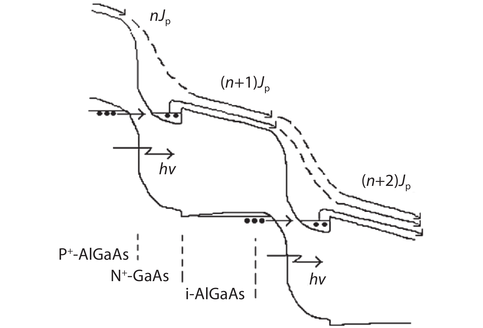
We proposed an improved structure to solve this problem. The working principle of the new infrared detector is presented in Fig. 4. As the picture shows, we inserted superlattices as the infrared absorption region after heavily doped PN junction, followed by a thick intrinsic barrier composed of i-AlGaAs. The tunnel compensated superlattice infrared detector separates depletion layers and quantum wells. The thickness of N+-GaAs layer in tunnel junction can be increased appropriately to prevent the expansion of the depletion layer. Compared with the original structure, the width of the quantum well is no longer influenced by the doping concentration of the tunnel junction. Thus, the sub-level of the quantum well can easily be controlled. This means that the effect of doping concentration error on device performance is reduced. In other words, the accuracy requirement of doping concentration is reduced. The difficulty of material growth is also reduced.
![]()
Figure 4.Schematic diagram of the improved structure under the reverse bias.
In an appropriate reverse bias, the ground state electrons of superlattices absorb photons jump to the excited state and across the barrier under the action of electric field. The photoelectrons are accelerated in the built-in potential field of the PN junction of the next cycle, passing through the next superlattice infrared absorption region at high speed. Meanwhile, the tunneling electrons from the p-GaAs valence band will fill into the empty quantum state of the ground state of the superlattices, reducing the recombination probability of photoelectrons.
Using a tunneling mechanism to fill empty quantum states can increase the photocurrent. This is a prerequisite for proper operation of the device. Therefore, the PN junction needs to be heavily doped to become a tunnel junction. The Fermi level in the n-region should be between the two subbands of the superlattices to ensure the injection efficiency of tunnel current into the ground state of superlattices. By measuring the peak voltage and the valley voltage of the tunnel junction, the Fermi level of the N region can be roughly estimated.
The superlattices are composed of wide and narrow band gap semiconductors that are periodically arranged. The barriers of superlattices need to be thin enough to form a tunnel resonance effect. Based on the tunneling resonance effect, the electrons traverse the barrier and fill the ground state of the superlattice. The position of the superlattice band is affected by the thickness of the well layer and the barrier layer and the barrier height. As soon as the structural parameters of the superlattice are determined, the absorption wavelength range of the device is determined. The transfer matrix method is a relatively simple and accurate method for calculating the position of subbands and the absorption wavelength.
The doping concentration of the superlattice should satisfy the condition that the electrons are sufficient to fill the ground state energy band and do not fill the excited state energy band. We designed the n-type doping concentration of the well to be 4 × 1017 cm–3 and the well width to be 6 nm. The calculated Fermi level[
![]()
Figure 5.The relationship between the gain and wavelength of different numbers of wells: (a) single well, (b) double well and (c) triple well.
3. Experiments and results
To verify the feasibility of the theory, we used MOCVD technology to grow an experimental sample. The sample has a photosensitive surface area of 200 × 200 μm2 and is optically coupled by 45° oblique incidence. It is a two-period structure, where each period contains a tunnel junction, a superlattice region with multiple wells and a thick intrinsic barrier. The structural parameters of the sample are shown in Table 1.
The response spectrum of the sample tested by Fourier transformation infrared spectrometer (FTIR) at 77 K is shown in Fig. 6. The device has a peak response wavelength of 7.73 μm. According to the transfer matrix method, the waveband that the device can absorb is about 7.48–8.93 μm, which is basically consistent with the test result.
![]()
Figure 6.Response spectrum of sample at 77 K.
Fig. 7 shows the dark current characteristics of the sample at different temperature. One negative differential resistance region is shown in Fig. 7(a) at positive bias. The position of the peak and the valley of the negative differential resistance region is 4.2 and 4.35 V, respectively, at low temperature. This indicates that the Fermi level above the conduction band of N+-GaAs 150 meV, approximately, is between the ground state and the first excited state in the superlattice region. This means that the empty quantum states generated by infrared radiation in ground state will be refilled by interband tunneling process. The reverse I–V curve is shown in Fig. 7(b). A small leakage current can be obtained when the reverse bias voltage is less than 1.1 V at 77 K. This is due to the unification of Fermi levels at zero bias, the close valence band of P+-GaAs, the conduction band of N+-GaAs, and the existence of large barriers in the device. To ensure the current transport, a large enough bias voltage must be applied to flatten the barrier. At this time, the photocurrent of the device can cross the barrier and the dark current is small enough. For a dual-period device sample, only one barrier needs to be flattened, so the optimal operating voltage of the device is 1.1 V.
![]()
Figure 7.Dark current versus applied bias of sample at 77 K. (a) Forward bias. (b) Reverse bias.
Fig. 8 shows the black body response test results of the device at 77 K. The blackbody temperature is 500 K. R represents the signal and N represents the noise. The maximum ratio of signal and noise is obtained when the reverse bias voltage is about 1.1 V. Simultaneously, the dark current is 2.99 × 10⁻⁸ A and the 500 K blackbody detectivity is 1.352 × 108 cm·Hz1/2·W–1. As voltage Vb continues to increase, the dark current of the device grows rapidly. This happens because the ground state electrons are more likely to tunnel through the barrier under large bias voltage. The experimental results of the original structure can be referred to Refs. [14, 16]. By comparison, it can be seen that the results of the two structures are similar.
![]()
Figure 8.Blackbody response test of sample at 77 K.
4. Conclusions
Based on the tunnel compensation multi-quantum well infrared detector, the superlattice layers are used as the infrared absorption region of the detector and the tunnel junctions provide tunnel compensation current for the superlattices, which are easy to fabricate by MOCVD technology. Experimental samples of two-period structure were fabricated using GaAs and AlGaAs materials, and the response spectrum, dark current characteristics and blackbody response of the device are obtained. The results show that the optimal operating voltage of the sample is 1.1 V, the dark current is 2.99 × 10⁻⁸ A, and the blackbody detectivity is 1.352 × 108 cm·Hz1/2·W–1 at 77 K. Owing to time constraints, detectors with more cycles have not been manufactured. In theory, however, detectors with more cycles can be expected to have larger photocurrents. The structural parameters of the device are subject to further optimization.
Acknowledgements
This work is supported by Beijing Natural Science Foundation (No. 4182011), the Development Foundation for Optoelectronics Technology Lab, Ministry of Education (No. PXM 2018_014204_500020), and National Natural Science Foundation of China (No. 61751502).
References
[1] A Rogalski. Recent progress in infrared detector technologies. Infrared Phys Technol, 54, 136(2011).
[2] H Kataria, C Asplund, A Lindberg et al. Novel high-resolution VGA QWIP detector. Proc SPIE, 10177(2017).
[3] K Roodenko, K K Choi, K P Clark et al. Control over the optical and electronic performance of GaAs/AlGaAs QWIPs grown by production MBE. Infrared Phys Technol, 84, 33(2017).
[4] M Jhabvala, K K Choi, C Monroy et al. Development of a 1 K × 1 K 8–12
[5] Y Kaya, A Ravikumar, G P Chen et al. Two-band ZnCdSe/ZnCdMgSe quantum well infrared photodetector. AIP Adv, 8, 075105(2018).
[6] Z F Li, Y L Jing, Y W Zhou. Multi-band integrated quantum well infrared photodetectors. International Conference on Infrared Millimeter and Terahertz Waves(2018).
[7] Y Wu, H M Liu, P Z Li. Dual-band quantum well infrared photodetector with metallic structure. Proc SPIE, 10697(2018).
[8] A Rogalski. Infrared detectors: an overview. Infrared Phys Technol, 43, 187(2002).
[9] T L Haran, J C James, S E Lane et al. Quantum efficiency and spatial noise tradeoffs for III–V focal plane arrays. Infrared Phys Technol, 97, 309(2019).
[10] S U Eker, M Hostut, Y Ergun et al. A new approach to quantum well infrared photodetectors: Staircase-like quantum well and barriers. Infrared Phys Technol, 48, 101(2006).
[11] K K Choi, S C Allen, J G Sun et al. Small pitch resonator-QWIP detectors and arrays. Infrared Phys Technol, 94, 118(2018).
[12] E A Jr DeCuir, K K Choi, J Sun et al. Progress in resonator quantum well infrared photodetector (R-QWIP) focal plane arrays. Infrared Phys Technol, 70, 138(2015).
[13] G X Su, L Liu, W B Zang et al. Highly efficient dielectric optical incoupler for quantum well infrared photodetectors. IEEE Photonics Technol Lett, 30, 1167(2018).
[14] J Deng, G D Shen, P Lian et al. Optoelectronic transport mechanism from subband infrared absorption and tunneling regeneration. Curr Appl Phys, 2, 373(2002).
[15] A Billaha, M K Das. Influence of doping on the performance of GaAs/AlGaAs QWIP for long wavelength applications. Opto−Electron Rev, 24, 25(2016).
[16] J Deng. Study on novel GaAs/AlGaAs multi-quantum wells infrared photodetecting mechanism and MOCVD epitaxy technology. Beijing: Beijing University of Technology, 79(2005).


Set citation alerts for the article
Please enter your email address

© Copyright 2018-2021 | Chinese Laser Press. All Rights Reserved 沪ICP备15018463号-20