• Photonics Research
  • Vol. 10, Issue 2, 357 (2022)
Zhihai Liu1、2, Siying Cheng1, Yu Zhang1、*, Wei Jin1, Xiang Li1, Yaru Li1, Yaxun Zhang1、4, Xinghua Yang1, Jianzhong Zhang1, and Libo Yuan3
Author Affiliations
  • 1Key Laboratory of In-fiber Integrated Optics, Ministry of Education, Harbin Engineering University, Harbin 150001, China
  • 2National Demonstration Center for Experimental Physics Education, Harbin Engineering University, Harbin 150001, China
  • 3Photonics Research Center, Guilin University of Electronics Technology, Guilin 541004, China
  • 4e-mail: zhangyaxun@hrbeu.edu.cn
  • show less
    DOI: 10.1364/PRJ.439506 Cite this Article Set citation alerts
    Zhihai Liu, Siying Cheng, Yu Zhang, Wei Jin, Xiang Li, Yaru Li, Yaxun Zhang, Xinghua Yang, Jianzhong Zhang, Libo Yuan. Intelligent all-fiber device: storage and logic computing[J]. Photonics Research, 2022, 10(2): 357 Copy Citation Text show less
    Operation principle of the all-fiber memory device. The fiber memory cell consists of fiber, GST, and ITO (as the capping layer). The information is stored in the phase state of GST and encoded as the GST’s reflectivity (amorphous state: logic state 0, low-reflectivity state; crystalline state: logic state 1, high-reflectivity state). Pump pulse (λ1=1550 nm) and probe light (λ2=1530 nm) into the optical fiber storage unit to write/erase and read the information.
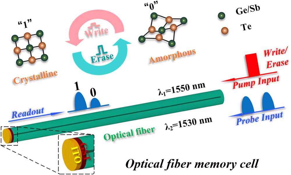
    Fig. 1. Operation principle of the all-fiber memory device. The fiber memory cell consists of fiber, GST, and ITO (as the capping layer). The information is stored in the phase state of GST and encoded as the GST’s reflectivity (amorphous state: logic state 0, low-reflectivity state; crystalline state: logic state 1, high-reflectivity state). Pump pulse (λ1=1550  nm) and probe light (λ2=1530  nm) into the optical fiber storage unit to write/erase and read the information.
    Scanning electron microscope (SEM) images of the all-fiber memory cell. (a) The SEM image of GST and ITO on the optical fiber end face; the optical fiber diameter is 125 μm. (b)–(d) The fiber end face has two layers of film structure (GST and ITO), and the thickness of GST and ITO is 120 nm and 30 nm, respectively.
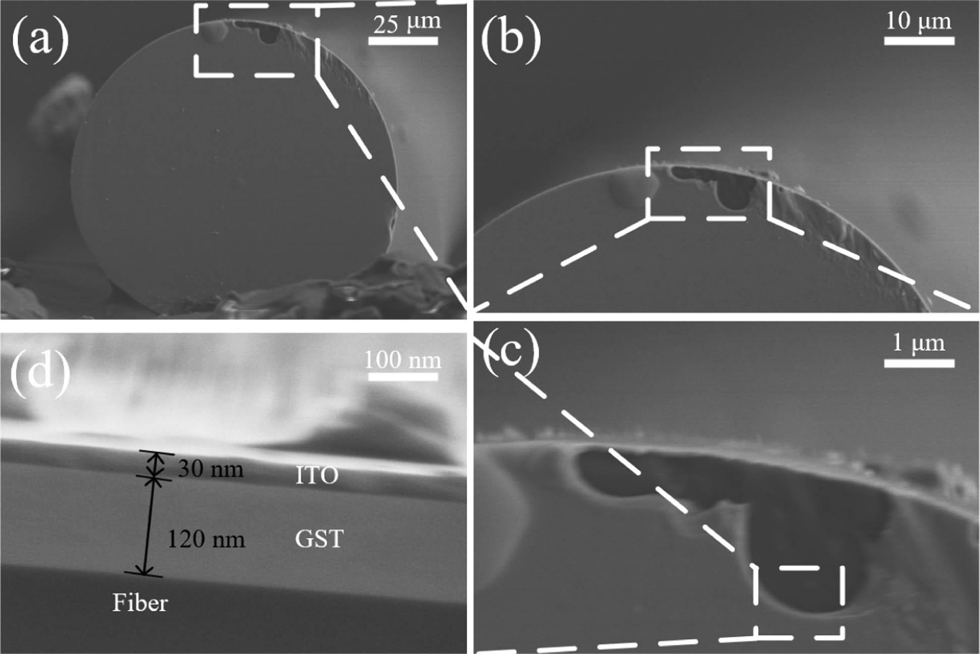
    Fig. 2. Scanning electron microscope (SEM) images of the all-fiber memory cell. (a) The SEM image of GST and ITO on the optical fiber end face; the optical fiber diameter is 125 μm. (b)–(d) The fiber end face has two layers of film structure (GST and ITO), and the thickness of GST and ITO is 120 nm and 30 nm, respectively.
    Simulated temperature distribution in the GST memory cell after a 10 ns programming pulse and simulated reflectivity and crystalline fraction as functions of power. The dark red region marks the area surpassing the melting temperature of GST (890 K). The optical reflectivity of GST increases (decreases) as the crystalline fraction increases (decreases). The inset shows the model diagram of pulsed light heating GST.
    Fig. 3. Simulated temperature distribution in the GST memory cell after a 10 ns programming pulse and simulated reflectivity and crystalline fraction as functions of power. The dark red region marks the area surpassing the melting temperature of GST (890 K). The optical reflectivity of GST increases (decreases) as the crystalline fraction increases (decreases). The inset shows the model diagram of pulsed light heating GST.
    Schematic of the optical measurement setup using probe/pump strategy. The pump laser (wavelength: λ1=1550 nm) and the probe laser in the CW mode (wavelength: λ2=1530 nm) are guided in/out of the memory cell. The output signal is filtered by a bandpass filter (BPF), connecting to a computer (PC) that monitors the reflectivity of the fiber memory at all times. The inset shows the rendered 3D picture of an all-fiber memory cell.
    Fig. 4. Schematic of the optical measurement setup using probe/pump strategy. The pump laser (wavelength: λ1=1550  nm) and the probe laser in the CW mode (wavelength: λ2=1530  nm) are guided in/out of the memory cell. The output signal is filtered by a bandpass filter (BPF), connecting to a computer (PC) that monitors the reflectivity of the fiber memory at all times. The inset shows the rendered 3D picture of an all-fiber memory cell.
    Measurements of multi-level operation using the PAM programming technique. (a) Experimental demonstration of eight different levels in the all-fiber device with the relative change in reflection (ΔR/Ri) recorded. A single pulse train with width W=10 ns is implemented to switch the photonic memory, and each level is reached by a determined optical power, from 54.5 to 47 mW. P1=54.5 mW, Pi=53.5, 52.5, 51.5, 50.5, 49.5, 48.5, 47 mW (i=2, 3, 4, 5, 6, 7, 8). (b) Multiple repetitions of the same switching cycle (levels 8 and 1) as in (a). Moreover, the 40 cycles verified a confidence interval of ±2.2%. (c) Accessing same levels but in random order featuring intra-level switching. Each level can also be independently reached and erased, with very accurate control of the reflection levels and remarkable repeatability. (d) Histogram plots of the difference between the desired reflectivity level and the actual reflectivity level. (e) Response time of a single pulse amorphization and crystallization; the time is 158 ns and 145 ns, respectively (the pulse width is 10 ns).
    Fig. 5. Measurements of multi-level operation using the PAM programming technique. (a) Experimental demonstration of eight different levels in the all-fiber device with the relative change in reflection (ΔR/Ri) recorded. A single pulse train with width W=10  ns is implemented to switch the photonic memory, and each level is reached by a determined optical power, from 54.5 to 47 mW. P1=54.5  mW, Pi=53.5, 52.5, 51.5, 50.5, 49.5, 48.5, 47 mW (i=2, 3, 4, 5, 6, 7, 8). (b) Multiple repetitions of the same switching cycle (levels 8 and 1) as in (a). Moreover, the 40 cycles verified a confidence interval of ±2.2%. (c) Accessing same levels but in random order featuring intra-level switching. Each level can also be independently reached and erased, with very accurate control of the reflection levels and remarkable repeatability. (d) Histogram plots of the difference between the desired reflectivity level and the actual reflectivity level. (e) Response time of a single pulse amorphization and crystallization; the time is 158 ns and 145 ns, respectively (the pulse width is 10 ns).
    Results of logical operation experiment. (a) Schematic of an optical logic device based on the fiber memory with two signal inputs Pin1 and Pin2 (Pin3 and Pin4). The “AND” gate is realized by using two storage logic units in series, and the “OR” gate is realized by combining the output signals of the two units with the coupler after two storage logic operation units are connected in parallel. (b) The normalized reflectivity outputs of the memlogic with different input combinations. The output is defined as logic “1” above the reference value. Moreover, the diagram on the left is the relationship between the input and output of the “AND” gate, and the diagram on the right is the relationship between the input and output of the “OR” gate. (c), (d) The truth table of the basic logic “AND,” “OR” calculation. Output at four different combinations of input states: (“1,” “1”); (“1,” “0”); (“0,” “1”); and (“0,” “0”).
    Fig. 6. Results of logical operation experiment. (a) Schematic of an optical logic device based on the fiber memory with two signal inputs Pin1 and Pin2 (Pin3 and Pin4). The “AND” gate is realized by using two storage logic units in series, and the “OR” gate is realized by combining the output signals of the two units with the coupler after two storage logic operation units are connected in parallel. (b) The normalized reflectivity outputs of the memlogic with different input combinations. The output is defined as logic “1” above the reference value. Moreover, the diagram on the left is the relationship between the input and output of the “AND” gate, and the diagram on the right is the relationship between the input and output of the “OR” gate. (c), (d) The truth table of the basic logic “AND,” “OR” calculation. Output at four different combinations of input states: (“1,” “1”); (“1,” “0”); (“0,” “1”); and (“0,” “0”).
    Zhihai Liu, Siying Cheng, Yu Zhang, Wei Jin, Xiang Li, Yaru Li, Yaxun Zhang, Xinghua Yang, Jianzhong Zhang, Libo Yuan. Intelligent all-fiber device: storage and logic computing[J]. Photonics Research, 2022, 10(2): 357
    Download Citation