
Zhihai Liu, Siying Cheng, Yu Zhang, Wei Jin, Xiang Li, Yaru Li, Yaxun Zhang, Xinghua Yang, Jianzhong Zhang, Libo Yuan, "Intelligent all-fiber device: storage and logic computing," Photonics Res. 10, 357 (2022)
- Photonics Research
- Vol. 10, Issue 2, 357 (2022)
Abstract
1. INTRODUCTION
In the era of fifth-generation (5G) mobile communication [1–3], optical fiber continues to play an essential role due to superfast transmission speed, tremendous bandwidth, and multiplexing capability in terms of wavelength [4]. With the rapid development of high-speed bandwidth services, higher requirements have been put forward for the optical fiber and transmission network’s functions, flexibility, and expansibility [5–7]. It requires the intelligent transformation in optical communication while realizing the large-capacity and ultra-high-speed transmission [8]. Therefore, we try to entrust optical fiber novel functions, storage, and computing, to serve intelligent optical communication more competently in addition to what we know about optical transmission function.
The common approaches to achieving light storage rely on either the bistability of artificial optical resonances [9–15] or the inherent bistable characteristics of devices stemming from their material properties [16–20]. These optical memories mainly rely on the master–slave configuration [9–12], the feedback loop scheme [13–15], or the injection-locking techniques [16–20], which have high integration density, short memory access time, and low-energy consumption. However, these devices are complex and volatile (extra energy is required to maintain the state of memory). Phase-change materials (PCMs) are ideal candidates for nonvolatile memories, which have large contrast in electrical/optical properties between the crystalline state and the amorphous state. They have been extensively studied and applied for electronic memories [21–26]. However, the “electronic rate bottleneck” of electronic memories limits modern computing technology development. All-optical memory based on PCMs can mitigate the von Neumann bottleneck with high speed and low power consumption in data transmission. The researchers use
Herein, we demonstrate all-fiber memory by combining the ordinary single-mode optical fiber (Corning SMF-28), GST, and indium-tin-oxide (ITO) (as the capping layer). Since GST has a significant contrast in optical reflectivity between the amorphous state (logic state 0, low-reflectivity state) and the crystalline state (logic state 1, high-reflectivity state), information is encoded as the reflectivity of the GST. It is stored in the phase state of GST. We use pump pulse (
Sign up for Photonics Research TOC. Get the latest issue of Photonics Research delivered right to you!Sign up now
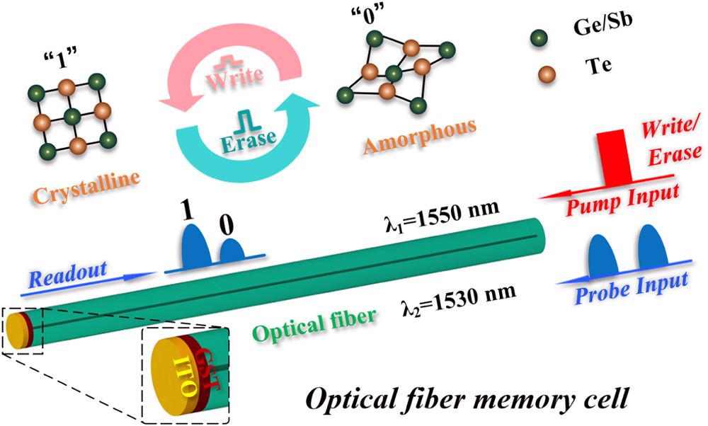
Figure 1.Operation principle of the all-fiber memory device. The fiber memory cell consists of fiber, GST, and ITO (as the capping layer). The information is stored in the phase state of GST and encoded as the GST’s reflectivity (amorphous state: logic state 0, low-reflectivity state; crystalline state: logic state 1, high-reflectivity state). Pump pulse (
2. PRINCIPLE
GST is a kind of chalcogenide phase-change material. It has a wide range of applications in near-infrared absorbers and modulators [39], data storage [40], and data calculation [41,42]. GST has two phases corresponding to the amorphous structure (a-GST) and cubic structure (c-GST). The two phases have very different material properties, thus providing the contrast requirements of distinguished logical states [43]. The GST can transform phases with electrical pulses or light pulses. People use significantly different electrical/optical properties in different phases to achieve data storage.
The scanning electron microscope images of our all-fiber memory cell are shown in Figs. 2(a)–2(d). The thicknesses of the GST and ITO are 120 nm and 30 nm, respectively. ITO prevents GST from being oxidized. Our all-fiber storage unit realizes optical storage by using the difference in reflectance between a-GST and c-GST. The scheme is the same as the principle used in conventional optical storage (where reflectivity is modulated). The crystalline state (which we term “level 1”) exhibits higher reflectivity than the amorphous state (“level 0”) [44,45]. Therefore, we define the conversion from a-GST to c-GST (crystallization) as the “write” process and the conversion from c-GST to a-GST (amorphization) as the “erase” process; the principle of GST transformation is shown in Fig. 1. We simulate a single 10 ns, 47 mW optical pulse train (the number is 100, and the repetition rate is 1 kHz) to heat GST to 580 K (see Fig. 3) to achieve the crystallization temperature of GST (500–600 K), and the 48.5 mW optical pulse can heat GST to an amorphous state, reaching the amorphous temperature of GST (890 K) [46].
![]()
Figure 2.Scanning electron microscope (SEM) images of the all-fiber memory cell. (a) The SEM image of GST and ITO on the optical fiber end face; the optical fiber diameter is 125 μm. (b)–(d) The fiber end face has two layers of film structure (GST and ITO), and the thickness of GST and ITO is 120 nm and 30 nm, respectively.
![]()
Figure 3.Simulated temperature distribution in the GST memory cell after a 10 ns programming pulse and simulated reflectivity and crystalline fraction as functions of power. The dark red region marks the area surpassing the melting temperature of GST (890 K). The optical reflectivity of GST increases (decreases) as the crystalline fraction increases (decreases). The inset shows the model diagram of pulsed light heating GST.
Multi-level storage requires the cell reflectivity to be programmed with higher accuracy as compared to bi-level storage. We must precisely control the crystal fraction of the active GST material to achieve the required cell reflectivity value with adequate accuracy [47]. We select a
3. RESULTS AND DISCUSSION
Our all-fiber memory device consists of a GST thin film passivated with a layer to prevent GST from oxidizing (ITO) and a single-mode fiber. GST is deposited on the end face of the fiber by radio frequency (RF) sputtering (50 W RF power, 30 mTorr Ar atmosphere, and
We use a pulsed laser (wavelength:
![]()
Figure 4.Schematic of the optical measurement setup using probe/pump strategy. The pump laser (wavelength:
The optical reflection of the a-GST is defined as the baseline; the pulse train (the number is 100 and the repetition rate is 1 kHz) with a fixed width of 10 ns and different peak power (
Here the powers of different optical pump pulses are
Levels 1 to 8 are sequentially achieved by decreasing the power from
![]()
Figure 5.Measurements of multi-level operation using the PAM programming technique. (a) Experimental demonstration of eight different levels in the all-fiber device with the relative change in reflection (
Level 6, for example, can be achieved from the level 1, 5, or 8 with the power of pump pulse of
We repeatedly switch GST states between levels 1 and 8 to further describe the storage performance. Figure 5(b) shows the result of repeated switching over 40 cycles, demonstrating that the all-optical data storage on the fiber end face has high repeatability. PCMs have operation cycles up to
We can use memory cells to manufacture all-fiber logic gates (“AND,” “OR”), which can meet the requirement of next-generation optical networks [52]. We name the present optical memory as “memlogic,” which is short for memory logic with both nonvolatile configurations of logic functions and nonvolatile logic output results [53].
Optical pulses of the power (
Figure 6(a) shows the logic operation principle of typical memlogic cells. First, as shown in Fig. 6(a), we connect two memlogic cells in series to perform the “AND” logic operation. Next, we connect two memlogic cells in parallel and combine two outputs with a coupler to achieve the “OR” logic operation. Each memlogic unit must be connected to a CIR because our all-fiber memory measures the reflection of the fiber. The reflectivities of two series memlogic units are defined as Rin1, Rin2, and the reflectivities of “OR” gate memlogic units are defined as Rin3, Rin4, respectively. According to the series and parallel characteristics of two memlogic units, the value of the reflectivity output after series (Rs) and parallel (Rp) connections can be expressed as
![]()
Figure 6.Results of logical operation experiment. (a) Schematic of an optical logic device based on the fiber memory with two signal inputs Pin1 and Pin2 (Pin3 and Pin4). The “AND” gate is realized by using two storage logic units in series, and the “OR” gate is realized by combining the output signals of the two units with the coupler after two storage logic operation units are connected in parallel. (b) The normalized reflectivity outputs of the memlogic with different input combinations. The output is defined as logic “1” above the reference value. Moreover, the diagram on the left is the relationship between the input and output of the “AND” gate, and the diagram on the right is the relationship between the input and output of the “OR” gate. (c), (d) The truth table of the basic logic “AND,” “OR” calculation. Output at four different combinations of input states: (“1,” “1”); (“1,” “0”); (“0,” “1”); and (“0,” “0”).
Importantly, when the logic inputs of
4. CONCLUSION
In summary, we have shown the demonstration of 3-bit data storage with an all-fiber memory cell. We use the PAM switching technique to realize partial crystallization of the PCM memory cell, and we can control the reflectivity in the GST layer by pulse power (
The results are a broad and fundamental step toward a fast, low-power fiber memory for applications. The all-fiber nonvolatile multi-level memory can have applications such as neuromorphic computing and in-memory computing. The primary logic gate is expected to realize more complex logic operations. The application of the memlogic unit in optical fiber communication networks is expected to lead to a new revolution in optical fiber communication technology.
Acknowledgment
Acknowledgment. The authors thank the College of Physics and Optoelectronic Engineering of Harbin Engineering University for providing technical support under the Key Laboratory of In-fiber Integrated Optics, Ministry of Education, China.
References
[1] T. Lagkas, D. Klonidis, P. Sarigiannidis, I. Tomkos. 5G/NGPON evolution and convergence: developing on spatial multiplexing of optical fiber links for 5G infrastructures. Fiber Integr. Opt., 39, 4-23(2020).
[2] S. Bjorn, B. Giulio, R. Ahmad, C. Fabio, O. Peter. Rethinking optical transport to pave the way for 5G and the networked society. J. Lightwave Technol., 33, 1084-1091(2015).
[3] J. S. Wey, J. W. Zhang. Passive optical networks for 5G transport: technology and standards. J. Lightwave Technol., 37, 2830-2837(2019).
[4] B. Lee. Review of the present status of optical fiber sensors. Opt. Fiber Technol., 9, 57-79(2003).
[5] D. Wang, Q. Sui, Z. Li. Toward universal optical performance monitoring for intelligent optical fiber communication networks. IEEE Commun. Mag., 58, 54-59(2020).
[6] P. Iovanna, F. Cavaliere, S. Stracca, L. Giorgi, F. Ubaldi. 5G xhaul and service convergence: transmission, switching and automation enabling technologies. J. Lightwave Technol., 38, 2799-2806(2020).
[7] G. Wellbrock, T. Wang, O. Ishida. New paradigms in optical communications and networks. IEEE Commun. Mag., 51, 22-23(2013).
[8] M. Naghshvarianjahromi, S. Kumar, M. J. Deen. Smart long-haul fiber optic communication systems using brain-like intelligence. 16th Canadian Workshop on Information Theory (CWIT), 1-6(2019).
[9] N. Pleros, D. Apostolopoulos, D. Petrantonakis, C. Stamatiadis, H. Avramopoulos. Optical static RAM cell. IEEE Photonics Technol. Lett., 21, 73-75(2009).
[10] D. Fitsios, C. Vagionas, G. T. Kanellos, A. Miliou, N. Pleros. Dual-wavelength bit input optical RAM with three SOA-XGM switches. IEEE Photonics Technol. Lett., 24, 1142-1144(2012).
[11] C. Vagionas, D. Fitsios, G. T. Kanellos, N. Pleros, A. Miliou. Optical RAM and flip-flops using bit-input wavelength diversity and SOA-XGM switches. J. Lightwave Technol., 30, 3003-3009(2012).
[12] M. Hill, H. Dorren, T. D. Vries, X. Leijtens, J. D. Besten, B. Smalbrugge, Y. Oei, H. Binsma, G. Khoe, M. Smit. A fast low-power optical memory based on coupled micro-ring lasers. Nature, 432, 206-209(2004).
[13] A. Trita, G. Mezõsi, M. Sorel, G. Giuliani. All-optical toggle flip-flop based on monolithic semiconductor ring laser. IEEE Photonics Technol. Lett., 26, 96-99(2014).
[14] P. Bakopoulos, K. Vyrsokinos, D. Fitsios, T. Alexoudi, D. Apostolopoulos, H. Avramopoulos, A. Miliou, N. Pleros. All-optical T-flip-flop using a single SOA-MZI-based latching element. IEEE Photonics Technol. Lett., 24, 748-750(2012).
[15] Y. Naito, S. Shimizu, T. Kato, K. Kobayashi, H. Uenohara. Investigation of all-optical latching operation of a monolithically integrated SOA-MZI with a feedback loop. Opt. Express, 20, B339-B349(2012).
[16] C. H. Chen, S. Matsuo, K. Nozaki, A. Shinya, M. Notomi. All-optical memory based on injection-locking bistability in photonic crystal lasers. Opt. Express, 19, 3387-3395(2011).
[17] J. Sakaguchi, T. Katayama, H. Kawaguchi. All-optical memory operation of 980-nm polarization bistable VCSEL for 20-Gb/s PRBS RZ and 40-Gb/s NRZ data signals. Opt. Express, 18, 12362-12370(2010).
[18] T. Katayama, T. Ooi, H. Kawaguchi. Experimental demonstration of multi-bit optical buffer memory using 1.55-μm polarization bistable vertical-cavity surface-emitting lasers. IEEE J. Quantum Electron., 45, 1495-1504(2009).
[19] D. Fitsios, T. Alexoudi, A. Bazin, P. Monnier, R. Raj, A. Miliou, G. T. Kanellos, N. Pleros, F. Raineri. Ultra-compact III–V-on-Si photonic crystal memory for flip-flop operation at 5 Gb/s. Opt. Express, 24, 4270-4277(2016).
[20] T. Alexoudi, D. Fitsios, G. Kanellos, A. Miliou, A. Bazin, R. Raj, F. Raineri, N. Pleros, P. Monnier. III-V-on-Si photonic crystal nanocavity laser technology for optical static random access memories. IEEE J. Sel. Top. Quantum Electron., 22, 4901410(2016).
[21] D. K. Loke, J. M. Skelton, T. H. Lee, R. Zhao, T. C. Chong, S. R. Elliott. Ultrafast nanoscale phase-change memory enabled by single-pulse conditioning. ACS Appl. Mater. Interfaces, 10, 41855-41860(2018).
[22] T. Matsunaga, J. Akola, S. Kohara, T. Honma, K. Kobayashi, E. Ikenaga, R. O. Jones, N. Yamada, M. Takata, R. Kojima. From local structure to nanosecond recrystallization dynamics in AgInSbTe phase-change materials. Nat. Mater., 10, 34-129(2011).
[23] M. Salinga, B. Kersting, I. Ronneberger, V. P. Jonnalagadda, X. T. Vu, M. L. Gallo, I. Giannopoulos, O. C. Mirédin, R. Mazzarello, A. Sebastian. Monatomic phase change memory. Nat. Mater., 17, 681-685(2018).
[24] W. Zhang, E. Ma. Single-element glass to record data. Nat. Mater., 17, 654-655(2018).
[25] F. Rao, K. Ding, Y. Zhou, Y. Zheng, M. Xia, S. Lv, Z. Song, S. Feng, I. Ronneberger, R. Mazzarello. Reducing the stochasticity of crystal nucleation to enable subnanosecond memory writing. Science, 358, 1423-1427(2017).
[26] G. M. Zewdie, Y. X. Zhou, L. Sun, F. Rao, V. L. Deringer, R. Mazzarello, W. Zhang. Chemical design principles for cache-type Sc-Sb-Te phase-change memory materials. Chem. Mater., 31, 4008-4015(2019).
[27] M. S. Arjunan, N. Saxena, A. Mondal, T. Dixit, A. Manivannan. High-stability and low-noise multi-level switching in In3SbTe2 material for phase change photonic memory applications. Phys. Status Solidi Rapid Res. Lett., 15, 2000354(2021).
[28] C. Zou, J. Zheng, C. Chang, A. Majumdar, L. Y. Lin. Nonvolatile rewritable photomemory arrays based on reversible phase-change perovskite for optical information storage. Adv. Opt. Mater., 7, 1900558(2019).
[29] W. H. P. Pernice, H. Bhaskaran. Photonic nonvolatile memories using phase change materials. Appl. Phys. Lett., 101, 171101(2012).
[30] C. Ríos, M. Stegmaier, P. Hosseini, D. Wang, T. Scherer, C. D. Wright, H. Bhaskaran, W. H. P. Pernice. Integrated all-photonic nonvolatile multi-level memory. Nat. Photonics, 9, 725-732(2015).
[31] E. Gemo, S. G. C. Carrillo, C. R. D. Galarreta, A. Baldycheva, C. D. Wright. Plasmonically-enhanced all-optical integrated phase-change memory. Opt. Express, 27, 24724-24737(2019).
[32] X. Li, N. Youngblood, C. Ríos, Z. G. Cheng, C. D. Wright, W. H. P. Pernice, H. Bhaskaran. Fast and reliable storage using a 5 bit, nonvolatile photonic memory cell. Optica, 6, 1-6(2019).
[33] Y. Zhang, J. B. Chou, J. Li, H. Li, Q. Du, A. Yadav, S. Zhou, M. Y. Shalaginov, Z. Fang, H. Zhong. Broadband transparent optical phase change materials for high-performance nonvolatile photonics. Nat. Commun., 10, 1(2019).
[34] M. S. Arjunan, A. Mondal, A. Das, K. V. Adarsh, A. Manivannan. Multi-level accumulative switching processes in growth-dominated AgInSbTe phase change material. Opt. Lett., 44, 3134-3137(2019).
[35] A. M. Sreekrishnan, A. Mondal, S. Durai, K. V. Adarsh, A. Manivannan. Impact of crystallization process in multi-level optical switching in Ge2Sb2Te5 and Ag5In5Sb60Te30 phase-change materials. J. Phys. D, 53, 495303(2020).
[36] Z. G. Cheng, C. Ríos, N. Youngblood, C. D. Wright, W. H. P. Pernice, H. Bhaskaran. Device‐level photonic memories and logic applications using phase‐change materials. Adv. Mater., 30, 1802435(2018).
[37] R. Marchetti, C. Lacava, L. Carroll, K. Gradkowski, P. Minzioni. Coupling strategies for silicon photonics integrated chips. Photon. Res., 7, 201-239(2019).
[38] H. J. S. Dorren, M. T. Hill, Y. Liu, N. Calabretta, A. Srivatsa, F. M. Huijskens, H. D. Waardt, G. D. Khoe. Optical packet switching and buffering by using all-optical signal processing methods. J. Lightwave Technol., 21, 2-12(2003).
[39] G. C. Carrillo, G. R. Nash, H. Hayat, J. C. Martin, K. Maciej, H. Bhaskaran, C. D. Wright. Design of practicable phase-change metadevices for near-infrared absorber and modulator applications. Opt. Express, 24, 13563-13573(2016).
[40] D. Lencer, M. Salinga, M. Wuttig. Design rules for phase-change materials in data storage applications. Adv. Mater., 23, 2030-2058(2011).
[41] C. Ríos, N. Youngblood, Z. Cheng, M. L. Gallo, W. H. P. Pernice, C. D. Wright, A. Sebastian, H. Bhaskaran. In-memory computing on a photonic platform. Sci. Adv., 5, eaau5759(2019).
[42] J. Feldmann, M. Stegmaier, N. Gruhler, C. Ríos, H. Bhaskaran, C. D. Wright, W. H. P. Pernice. Calculating with light using a chip-scale all-optical abacus. Nat. Commun., 8, 1256(2017).
[43] S. Abdollahramezani, O. Hemmatyar, H. Taghinejad, A. Krasnok, A. Adibi. Tunable nanophotonics enabled by chalcogenide phase-change materials. Nanophotonics, 9, 1189-1241(2020).
[44] L. Wang, L. Tu, J. Wen. Application of phase-change materials in memory taxonomy. Sci. Technol. Adv. Mater., 18, 406-429(2017).
[45] J. Siegel, A. Schropp, J. Solis, C. N. Afonso, M. Wuttig. Rewritable phase-change optical recording in Ge2Sb2Te5 films induced by picosecond laser pulses. Appl. Phys. Lett., 84, 2250-2252(2004).
[46] N. Yamada, E. Ohno, K. Nishiuchi, N. Akahira, M. Takao. Rapid‐phase transitions of GeTe‐Sb2Te3 pseudobinary amorphous thin films for an optical disk memory. J. Appl. Phys., 69, 2849-2856(1991).
[47] E. Kuramochi, M. Notomi. Phase-change memory. Nat. Photonics, 9, 712-714(2015).
[48] Y. G. Chen, X. Li, Y. Sonnefraud, I. F. D. Antonio, X. G. Luo, M. H. Hong, S. A. Maier. Engineering the phase front of light with phase-change material based planar lenses. Sci. Rep., 5, 8660(2015).
[49] N. V. Voshchinnikov, G. Videen, T. Henning. Effective medium theories for irregular fluffy structures: aggregation of small particles. Appl. Opt., 46, 4065-4072(2007).
[50] C. Rios, M. Stegmaier, Z. G. Cheng, N. Youngblood, C. D. Wright, W. H. P. Pernice, H. Bhaskaran. Controlled switching of phase-change materials by evanescent-field coupling in integrated photonics. Opt. Mater. Express, 8, 2455-2470(2018).
[51] M. Stegmaier, C. Rios, P. Hosseini, C. D. Wright, H. Bhaskaran, W. H. P. Pernice. All-photonic nonvolatile memory cells using phase-change materials. IEEE Photonics Conference, 484-485(2015).
[52] J. Y. Tian, H. Luo, Y. Q. Yang, F. Ding, Y. R. Qu, D. Zhao, M. Qiu, S. I. Bozhevolnyi. Active control of anapole states by structuring the phase-change alloy Ge2Sb2Te5. Nat. Commun., 10, 396(2019).
[53] H. W. Tan, G. Liu, H. L. Yang, X. H. Yi, L. Pan, J. Shang, S. B. Long, M. Liu, Y. H. Wu, R. W. Li. Light-gated memristor with integrated logic and memory functions. ACS Nano, 11, 11298-11305(2017).


Set citation alerts for the article
Please enter your email address

© Copyright 2018-2021 | Chinese Laser Press. All Rights Reserved 沪ICP备15018463号-20