• Journal of Infrared and Millimeter Waves
  • Vol. 40, Issue 5, 569 (2021)
Xiao-Le MA1, Jie GUO1、*, Rui-Ting HAO1, Guo-Shuai WEI1, Guo-Wei WANG2、3, Ying-Qiang XU2、3, and Zhi-Chuan NIU2、3
Author Affiliations
  • 1Yunnan Key Laboratory of Opto-Electronic Information Technology,Yunnan Normal University,Kunming 650500,China
  • 2State Key Laboratory for Superlattices and Microstructures,Institute of Semiconductors,Chinese Academy of Sciences,Beijing 100083,China
  • 3Center of Materials Science and Optoelectronics Engineering,University of Chinese Academy of Sciences,Beijing 100049,China
  • show less
    DOI: 10.11972/j.issn.1001-9014.2021.05.001 Cite this Article
    Xiao-Le MA, Jie GUO, Rui-Ting HAO, Guo-Shuai WEI, Guo-Wei WANG, Ying-Qiang XU, Zhi-Chuan NIU. Mid-/Short-Wave dual-band infrared detector based on InAs/GaSb superlattice /GaSb bulk materials[J]. Journal of Infrared and Millimeter Waves, 2021, 40(5): 569 Copy Citation Text show less
    Structure diagram of mid-/short-wave dual-band infrared detector based on InAs/GaSb superlattice/GaSb bulk material
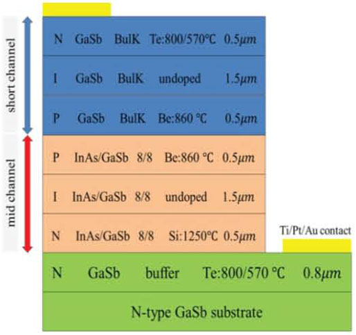
    Fig. 1. Structure diagram of mid-/short-wave dual-band infrared detector based on InAs/GaSb superlattice/GaSb bulk material
    Schematic diagram of process flow
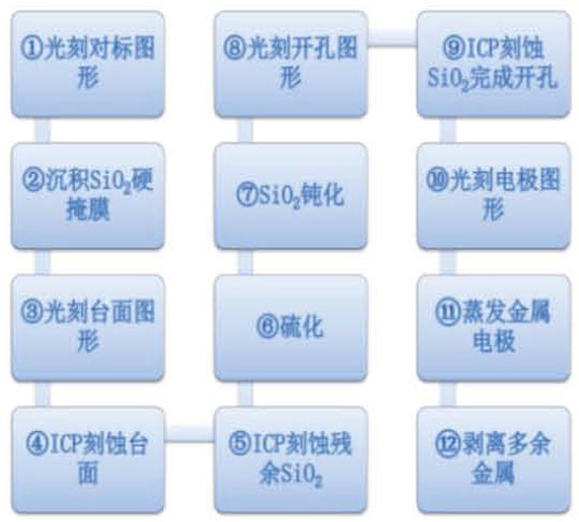
    Fig. 2. Schematic diagram of process flow
    Schematic diagram of device vertical profile(a)Anodic sulfuration+passivation,(b)direct SiO2 passivation
    Fig. 3. Schematic diagram of device vertical profile(a)Anodic sulfuration+passivation,(b)direct SiO2 passivation
    High-resolution X-ray diffraction(HRXRD)image of the device
    Fig. 4. High-resolution X-ray diffraction(HRXRD)image of the device
    Optical microscope image of the sample surface (a) AFM image of the surface (b) and SEM image of the section(c)
    Fig. 5. Optical microscope image of the sample surface (a) AFM image of the surface (b) and SEM image of the section(c)
    Curve of dark current density J and R∙A at different temperatures vs bias for sulfurized +SiO2 passivated devices(a)and(c)and SiO2 passivated devices(b)and(d)
    Fig. 6. Curve of dark current density J and R∙A at different temperatures vs bias for sulfurized +SiO2 passivated devices(a)and(c)and SiO2 passivated devices(b)and(d)
    Curves of the dark current density(a)and R∙A value(b)of the device varying with temperature under bias voltage of -100 mV
    Fig. 7. Curves of the dark current density(a)and R∙A value(b)of the device varying with temperature under bias voltage of -100 mV
    The data of R0A changing with P/A value of devices with different mesa area at 77 K and its fitting curve
    Fig. 8. The data of R0A changing with P/A value of devices with different mesa area at 77 K and its fitting curve
    Normalized spectral response curve of the device(a)short wave channel,(b)middle wave channel
    Fig. 9. Normalized spectral response curve of the device(a)short wave channel,(b)middle wave channel
    Blackbody spectral responsivity curve of the device
    Fig. 10. Blackbody spectral responsivity curve of the device
    Xiao-Le MA, Jie GUO, Rui-Ting HAO, Guo-Shuai WEI, Guo-Wei WANG, Ying-Qiang XU, Zhi-Chuan NIU. Mid-/Short-Wave dual-band infrared detector based on InAs/GaSb superlattice /GaSb bulk materials[J]. Journal of Infrared and Millimeter Waves, 2021, 40(5): 569
    Download Citation