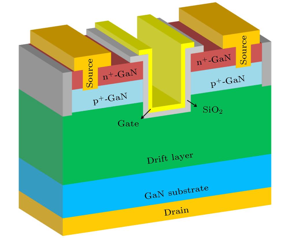

Fu Chen, Wen-Xin Tang, Guo-Hao Yu, Li Zhang, Kun Xu, Bao-Shun Zhang. Effect of U-shape trench etching process on electrical properties of GaN vertical trench metal-oxide-semiconductor field-effect transistor [J]. Acta Physica Sinica, 2020, 69(9): 098501-1
- Acta Physica Sinica
- Vol. 69, Issue 9, 098501-1 (2020)
Abstract

Set citation alerts for the article
Please enter your email address
© Copyright 2018-2021 | Chinese Laser Press. All Rights Reserved 沪ICP备15018463号-20