[1] Ohtsu M.Near-Field Nano/Atom Optics and Technology(Springer, Berlin, 1998).
[2] Zhu X, Ohtsu M.Near-Field Optics: Principles and Applications(World Scientific, Singapore, 2000).
[3] M Ohtsu. From classical to modern near-field optics and the future. Opt Rev, 21, 905-910(2014).
[4] E H Synge. A suggested method for extending microscopic resolution into the ultra-microscopic region. Lond Edinb Dublin Phil Mag J Sci, 6, 356-362(1928).
[5] J A O'Keefe. Resolving power of visible light. J Opt Soc Am, 46, 359(1956).
[6] H A Bethe. Theory of diffraction by small holes. Phys Rev, 66, 163-182(1944).
[7] C J Bouwkamp. On the diffraction of electromagnetic waves by small circular disks and holes. Philips Res Rep, 5, 401-422(1950).
[8] E A Ash, G Nicholls. Super-resolution aperture scanning microscope. Nature, 237, 510-512(1972).
[9] Pohl D W, Courjon D.Near Field Optics (Kluwer, Dordrecht, 1993).
[10] D W Pohl, W Denk, M Lanz. Optical stethoscopy:image recording with resolution λ/20. Appl Phys Lett, 44, 651-653(1984).
[11] A Lewis, M Isaacson, A Harootunian, A Muray. Development of a 500Å spatial resolution light microscope:I.Light is efficiently transmitted through λ/16 diameter apertures. Ultramicroscopy, 13, 227-231(1984).
[12] U C Fischer. Optical characteristics of 0.1μm circular apertures in a metal film as light sources for scanning ultramicroscopy. J Vac Sci Technol B, 3, 386-390(1985).
[13] E Betzig, M Isaacson, A Lewis. Collection mode near-field scanning optical microscopy. Appl Phys Lett, 51, 2088-2090(1987).
[14] Mononobe S, Saiki T.Chs 3 and 4 in Near-Field Nano/Atom Optics and Technol .(ed Ohtsu M.Springer Tokyo, 1998).
[15] E Betzig, J K Trautman, T D Harris, J S Weiner, R L Kostelak. Breaking the diffraction barrier:optical microscopy on a nanometric scale. Science, 251, 1468-1470(1991).
[16] T Pangaribuan, K Yamada, S D Jian, H Ohsawa, M Ohtsu. Reproducible fabrication technique of nanometric tip diameter fiber probe for photon scanning tunneling microscope. Jpn J Appl Phys, 31, L1302-L1304(1992).
[17] L Malmqvist, H M Hertz. Trapped particle optical microscopy. Opt Commun, 94, 19-24(1992).
[18] N F van Hulst, M H P Moers, O F J Noordman, R G Tack, F B Segerink et al. Near-field optical microscope using a silicon-nitride probe. Appl Phys Lett, 62, 461-463(1993).
[19] F Zenhausern, Y Martin, H K Wickramasinghe. Scanning interferometric apertureless microscopy:optical imaging at 10 angstrom resolution. Science, 269, 1083-1085(1995).
[20] J M Guerra. Photon tunneling microscopy. Appl Opt, 29, 3741-3752(1990).
[21] E Betzig, R J Chichester. Single molecules observed by near-field scanning optical microscopy. Science, 262, 1422-1425(1993).
[22] X S Xie, R C Dunn. Probing single molecule dynamics. Science, 265, 361-364(1994).
[23] R U Maheswari, S Mononobe, H Tatsumi, Y Katayama, M Ohtsu. Observation of subcellular structures of neurons by an illumination mode near-field optical microscope under an optical feedback control. Opt Rev, 3, 463-467(1996).
[24] J Levy, V Nikitin, J M Kikkawa, D D Awschalom, N Samarth. Femtosecond near-field spin microscopy in digital magnetic heterostructures. J Appl Phys, 79, 6095-6100(1996).
[25] T Saiki, K Nishi, M Ohtsu. Low temperature near-field photoluminescence spectroscopy of InGaAs single quantum dots. J Appl Phys, 37, 1638-1642(1998).
[26] Y Narita, H Murotani. Submicrometer optical characterization of the grain boundary of optically active Cr3+ doped polycrystalline Al2O3 by near-field spectroscopy. Am Mineral, 87, 1144-1147(2002).
[27] M Isaacson, J Cline, H Barshatzky. Resolution in near-field optical microscopy. Ultramicroscopy, 47, 15-22(1992).
[28] E Wolf, M Nieto-Vesperinas. Analyticity of the angular spectrum amplitude of scattered fields and some of its consequences. J Opt Soc Am, 2, 886-890(1985).
[29] C Girard, D Courjon. Model for scanning tunneling optical microscopy:a microscopic self-consistent approach. Phys Rev B, 42, 9340-9439(1990).
[30] Eah S K, Jhe W, Saiki T, Ohtsu M.Study of quantum optical effects with scanning near-field optical microscopy In Proceedings of theFirstAsia-PacificWorkshoponNearFieldOptics(1996).
[31] K Kobayashi, M Ohtsu. Quantum theoretical approach to a near-field optical system. J Microsc, 194, 249-254(1999).
[32] K Kobayashi, S Sangu, H Ito, M Ohtsu. Near-field optical potential for a neutral atom. Phys Rev A, 63, 013806(2001).
[33] H Ito, T Nakata, K Sakaki, M Ohtsu, K I Lee et al. Laser spectroscopy of atoms guided by evanescent waves in micron-sized hollow optical fibers. Phys Rev Lett, 76, 4500-4503(1996).
[34] M Ohtsu, K Kobayashi, T Kawazoe, S Sangu, T Yatsui. Nanophotonics:design, fabrication, and operation of nanometric devices using optical near fields. IEEE J Sel Top Quantum Electron, 8, 839-862(2002).
[35] Ohtsu M.Handbook of Nano-Optics and Nanophotonics (Springer, Heidelberg, New York, 2013).
[36] Ohtsu M, Yatsui T.Progress in Nanophotonics 4(Springer, Heidelberg, 2017).
[37] Y Tanaka, K Kobayashi. Spatial localization of an optical near field in one-dimensional nanomaterial system. Physica E, 40, 297-300(2007).
[38] S Sangu, K Kobayashi, M Ohtsu. Optical near fields as photon-matter interacting systems. J Microsc, 202, 279-285(2001).
[39] S A Maier, M L Brongersma, P G Kik, S Meltzer, A A G Requicha et al. Plasmonics—A route to nanoscale optical devices. Adv Mater, 13, 1501-1505(2001).
[40] S Sangu, K Kobayashi, S Shojiguchi, M Ohtsu. Logic and functional operations using a near-field optically coupled quantum-dot system. Phys Rev B, 69, 115334(2004).
[41] T Kawazoe, M Ohtsu, S Aso, Y Sawado, Y Hosoda et al. Two-dimensional array of room-temperature nanophotonic logic gates using InAs quantum dots in mesa structures. Appl Phys B, 103, 537-546(2011).
[42] T Kawazoe, S Tanaka, M Ohtsu. Single-photon emitter using excitation energy transfer between quantum dots. J Nanophoton, 2, 029502(2008).
[43] M Naruse, P Holmström, T Kawazoe, K Akahane, N Yamamoto et al. Energy dissipation in energy transfer mediated by optical near-field interactions and their interfaces with optical far-fields. Appl Phys Lett, 100, 241102(2012).
[44] M Naruse, K Leibnitz, F Peper, N Tate, W Nomura et al. Autonomy in excitation transfer via optical near-field interactions and its implications for information networking. Nano Commun Netw, 2, 189-195(2011).
[45] M Naruse, N Tate, M Aono, M Ohtsu. Information physics fundamentals of nanophotonics. Rep Prog Phys, 76, 056401(2013).
[46] S J Kim, M Naruse, M Aono, M Ohtsu, M Hara. Decision maker based on nanoscale photo-excitation transfer. Sci Rep, 3, 2370(2013).
[47] M Aono, M Naruse, S J Kim, M Wakabayashi, H Hori et al. Amoeba-inspired nanoarchitectonic computing:solving intractable computational problems using nanoscale photoexcitation transfer dynamics. Langmuir, 29, 7557-7564(2013).
[48] N Tate, H Sugiyama, M Naruse, W Nomura, T Yatsui et al. Quadrupole-dipole transform based on optical near-field interactions in engineered nanostructures. Opt Express, 17, 11113-11121(2009).
[49] N Tate, M Naruse, T Yatsui, T Kawazoe, M Hoga et al. Nanophotonic code embedded in embossed hologram for hierarchical information retrieval. Opt Express, 18, 7497-7505(2010).
[50] T Kawazoe, K Kobayashi, S Takubo, M Ohtsu. Nonadiabatic photodissociation process using an optical near field. J Chem Phys, 122, 024715(2005).
[51] T Kawazoe, K Kobayashi, M Ohtsu. Near-field optical chemical vapor deposition using Zn (acac)2 with a non-adiabatic photochemical process. Appl Phys B, 84, 247-251(2006).
[52] http://doi.org/10.14939/1802R.001.v1.
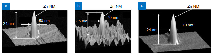
[53] J Lim, T Yatsui, M Ohtsu. Observation of size-dependent resonance of near-field coupling between a deposited Zn dot and the probe apex during near-field optical chemical vapor deposition. IEICE Trans Electron E88-C(1832).
[54] Kobayashi K, Sangu S, Ohtsu M, Ch 5 in Progress in Nano-Electro-Optics(Springer, Heidelberg, 2003).
[55] V V Polonski, Y Yamamoto, M Kourogi, H Fukuda, M Ohtsu. Nanometric patterning of zinc by optical near-field photochemical vapour deposition. J Microsc, 194, 545-551(1999).
[56] H Yonemitsu, T Kawazoe, K Kobayashi, M Ohtsu. Nonadiabatic photochemical reaction and application to photolithography. J Luminesc, 122-123, 230-233(2007).
[57] Y Inao, S Nakasato, R Kuroda, M Ohtsu. Near-field lithography as prototype nano-fabrication tool. Microelectron Eng, 84, 705-710(2007).
[58] T Kawazoe, K Kobayashi, K Akahane, M Naruse, N Yamamoto et al. Demonstration of nanophotonic NOT gate using near-field optically coupled quantum dots. Appl Phys B, 84, 243-246(2006).
[59] T Kawazoe, T Takahashi, M Ohtsu. Evaluation of the dynamic range and spatial resolution of nonadiabatic optical near-field lithography through fabrication of Fresnel zone plates. Appl Phys B, 98, 5-11(2010).
[60] Koike M, Miyauchi S, Sano K, Imazono T.Ch.9 in Nanophotonics and Nanofabrication.(ed Ohtsu M.Wiley-VCH, 2009).
[61] K Hirata. Realization of high-performance optical element by optical near-field etching. Proc SPIE, 7921, 9210M(2011).
[62] T Yatsui, W Nomura, M Ohtsu. Realization of ultraflat plastic film using dressed-photon-phonon-assisted selective etching of nanoscale structures. Adv Opt Technol, 2015, 701802(2015).
[63] D W Allan. Statistics of atomic frequency standards. Proc IEEE, 54, 221-230(1966).
[64] T Yatsui, K Hirata, T Tabata, Y Miyake, Y Akita et al. Self-organized near-field etching of the sidewalls of glass corrugations. Appl Phys B, 103, 527-530(2011).
[65] R Teki, Kadaksham A John, M House, J Harris-Jones, A Ma et al. Alternative smoothing techniques to mitigate EUV substrate defectivity. Proc SPIE, 8322, 83220B(2012).
[66] T Yatsui, W Nomura, F Stehlin, O Soppera, M Naruse et al. Challenges in realizing ultraflat materials surfaces. Beilstein J Nanotechnol, 4, 875-885(2013).
[67] W Nomura, T Yatsui, Y Yanase, K Suzuki, M Fujita et al. Repairing nanoscale scratched grooves on polycrystalline ceramics using optical near-field assisted sputtering. Appl Phys B, 99, 75-78(2010).
[68] T Yatsui, W Nomura, M Naruse, M Ohtsu. Realization of an atomically flat surface of diamond using dressed photon-phonon etching. J Phys D, 45, 475302(2012).
[69] T Kawazoe, H Fujiwara, K Kobayashi, M Ohtsu. Visible light emission from dye molecular grains via infrared excitation based on the nonadiabatic transition induced by the optical near field. IEEE J Sel Top Quant Electron, 15, 1380-1386(2009).
[70] H Fujiwara, T Kawazoe, M Ohtsu. Nonadiabatic multi-step excitation for the blue-green light emission from dye grains induced by the near-infrared optical near-field. Appl Phys B, 98, 283-289(2010).
[71] H Fujiwara, T Kawazoe, M Ohtsu. Nonadiabatic nondegenerate excitation by optical near-field and its application to optical pulse-shape measurement. Appl Phys B, 100, 85-91(2010).
[72] N Tate, M Naruse, Y Liu, T Kawazoe, T Yatsui et al. Experimental demonstration and stochastic modeling of autonomous formation of nanophotonic droplets. Appl Phys B, 112, 587-592(2013).
[73] Yatsui T.Progress in Nanophotonics 5(Springer, 2018).
[74] S Yukutake, T Kawazoe, T Yatsui, W Nomura, K Kitamura et al. Selective photocurrent generation in the transparent wavelength range of a semiconductor photovoltaic device using a phonon-assisted optical near-field process. Appl Phys B, 99, 415-422(2010).
[75] H Tanaka, T Kawazoe, M Ohtsu. Increasing Si photodetector photosensitivity in near-infrared region and manifestation of optical amplification by dressed photons. Appl Phys B, 108, 51-56(2012).
[76] K D Hirschman, L Tsybeskov, S P Duttagupta, P M Fauchet. Silicon-based visible light-emitting devices integrated into microelectronic circuits. Nature, 384, 338-341(1996).
[77] Z H Lu, D J Lockwood, J M Baribeau. Quantum confinement and light emission in SiO2/Si superlattices. Nature, 378, 258-260(1995).
[78] M M Milosevic, X Chen, W Cao, A F J Runge, Y Franz et al. Ion implantation in silicon for trimming the operating wavelength of ring resonators. IEEE J Sel Top Quant Electron, 24, 8200107(2018).
[79] T Kawazoe, M A Mueed, M Ohtsu. Highly efficient and broadband Si homojunction structured near-infrared light emitting diodes based on the phonon-assisted optical near-field process. Appl Phys B, 104, 747-754(2011).
[80] J H Kim, T Kawazoe, M Ohtsu. Optimization of dressed-photon—phonon-assisted annealing for fabricating GaP light-emitting diodes. Appl Phys A, 121, 1395-1401(2015).
[81] M Yamaguchi, T Kawazoe, M Ohtsu. Evaluating the coupling strength of electron-hole pairs and phonons in a 0.9μm-wavelength silicon light emitting diode using dressed-photon-phonons. Appl Phys A, 115, 119-125(2014).
[82] N Wada, M A Tran, T Kawazoe, M Ohtsu. Measurement of multimode coherent phonons in nanometric spaces in a homojunction-structured silicon light emitting diode. Appl Phys A, 115, 113-118(2014).
[83] M Ohtsu, T Kawazoe. Principles and practices of Si light emitting diodes using dressed photons. Adv Mater Lett, 10, 860-867(2019).
[84] Y Tanaka, K Kobayashi. Optical near field dressed by localized and coherent phonons. J Microsc, 229, 228-232(2008).
[85] T Kawazoe, K Nishioka, M Ohtsu. Polarization control of an infrared silicon light-emitting diode by dressed photons and analyses of the spatial distribution of doped boron atoms. Appl Phys A, 121, 1409-1415(2015).
[86] M A Tran, T Kawazoe, M Ohtsu. Fabrication of a bulk silicon p-n homojunction-structured light-emitting diode showing visible electroluminescence at room temperature. Appl Phys A, 115, 105-111(2014).
[87] M Yamaguchi, T Kawazoe, T Yatsui, M Ohtsu. Spectral properties of a lateral p-n homojunction-structured visible silicon light-emitting diode fabricated by dressed-photon—phonon-assisted annealing. Appl Phys A, 121, 1389-1394(2015).
[88] Ohtsu M.Silicon Light-Emitting Diodes and Lasers(Springer, Heidelberg, 2016).
[89] T Kawazoe, M Ohtsu, K Akahane, N Yamamoto. Si homojunction structured near-infrared laser based on a phonon-assisted process. Appl Phys B, 107, 659-663(2012).
[90] Kawazoe T.High power Silicon laser based on the dressed photon technology.In Proceedings of 2017 International Conference on Solid State Devices and Materials 413-414(2017).
[91] Ohtsu M, Ojima I, Sakuma H.Ch 1, Vol 62 in Progress in Optics(ed Visser T.Elsevier, 2019)
[92] Ohtsu M.Ch 6 and Ch 8 in Silicon Light-Emitting Diodes and Lasers(Springer, Heidelberg, 2016).
[93] N Tate, T Kawazoe, W Nomura, M Ohtsu. Current-induced giant polarization rotation using a ZnO single crystal doped with nitrogen ions. Sci Rep, 5, 12762(2015).
[94] T D Newton, E P Wigner. Localized states for elementary systems. Rev Mod Phys, 21, 400-406(1949).
[95] Ojima I.Micro-macro duality in quantum physics.Ch 12 in Stochastic Analysis: Classical and Quantum-Perspectives of White Noise Theory(ed T Hida.World Scientific, 2005).
[96] Ojima I.Nakanishi-Lautrup, B-field, crossed product and duality.In ResearchonQuantumFieldTheory, RIMSWorkshop(2006).
[97] G F Dell'Antonio. Support of a field in p space. J Math Phys, 2, 759-766(1961).
[98] Y Aharonov, A Komar, L Susskind. Superluminal behavior, causality, and instability. Phys Rev, 182, 1400-1403(1969).
[99] Yatsui T.Vol 5 in Progress in Nanophotonics(Springer, 2018). [100.Ohtsu M, Ojima I, Sakuma H.Ch 2, Vol 64 in Progress in Optics(ed Visser T D.Elsevier, 2019).
[100] Ohtsu M, Ojima I, Sakuma H. Ch 2, Vol 64 in Progress in Optics (ed Visser T D. Elsevier, 2019).