
Motoichi Ohtsu. History, current developments, and future directions of near-field optical science[J]. Opto-Electronic Advances, 2020, 3(3): 190046-1
- Opto-Electronic Advances
- Vol. 3, Issue 3, 190046-1 (2020)
Abstract
Introduction
The relatively new optical science of dressed photons (DPs) has seen rapid progress recently. The DP is a quantum field created in a complex system composed of photons and electrons (or excitons) in a nanometer-sized material. The fruits of this science have been applied to develop generic technologies (for example, nanometer-sized optical devices, information processing systems using these devices, nano-fabrication technology, and energy conversion technology) to realize disruptive innovations. Furthermore, studies on off-shell science have commenced. Off-shell science is a novel optical science including studies on the DP. The origin of this science can be found in near-field optics, which was actively investigated in the 1980s and 1990s after a long period of incubation since the 1920s. Studies on near-field optics started with the aim of achieving disruptive innovations in optical science, especially in optical microscopy. Extensive studies were carried out in the 1980s and 1990s, and they have mostly already come to an end. However, basic studies exploring the nature of the optical near field (ONF) were steadily continued by a small number of scientists, and near-field optics was reincarnated as a novel science of the DP. This science involves the study of light-matter interactions in a nanometer-sized space and explores novel applications that are contrary to those in conventional optical science and technology.
The author of this paper (M.O.) has been engaged in work on near-field optics for over three decades, spurred by a simple and intuitive desire to miniaturize the dimensions of light
History
To start a review on the history of near-field optics, first, the principles of creating and detecting the ONF should be explained: Scattered light is created when a nanometer-sized material (NM1) is illuminated by light. It should be noted that another form of electromagnetic field is also created in NM1 or on its surface. This field is called the ONF. The ONF is localized on NM1, and its spatial extent (size) is equivalent to the size of NM1. The ONF cannot be detected by a conventional photodetector installed far from NM1 because it does not propagate to the far field. To detect it, a second nanometer-sized material (NM2) is inserted into the ONF. The ONF is disturbed by NM2 and is converted to scattered light that propagates to the far field, and is thus detected by a photodetector.
Since the size of the ONF is equivalent to the size of NM1, it is expected that one can use the ONF to break through the diffraction limit which determines the spatial resolution in optical microscopy. In such a system, the ONF on NM1 works as a light source for acquiring an optical microscope image of NM2. Based on this expectation, research on near-field optics was started with the aim of realizing this breakthrough, and a great deal of effort was made to create an ONF whose size Δx is much smaller than the wavelength λ of light (Δx < < λ).
Since conventional optical theories were used in the early studies on near-field optics, the momentum p of the electromagnetic field has been treated as a definite quantity even though it is accompanied by a small uncertainty Δp due to quantum fluctuations. However, it should be pointed out that Heisenberg's uncertainty principle Δp·Δx≥h/2π (where h is Planck's constant) indicates a large uncertainty Δp (Δp > > p) because of the relation Δx < < λ above.
Modern studies are treating the ONF as a quantum field with a large energy uncertainty ΔE as well as a large Δp. In particular, by examining the light-matter interactions in nanometer-sized spaces, a variety of novel phenomena that are contrary to those in conventional optical phenomena have been discovered. That is to say, near-field optics was reincarnated as a novel optical science, and the ONF was renamed the DP. Taking note of this reincarnation, the history of near-field optics is reviewed in the following.
It has been recognized that the classical period of near-field optics started in the 1920s to 1950s, with proposals that it be applied to high-resolution optical microscopy to achieve resolutions beyond the diffraction limit
In the 1980s and 1990s, experimental demonstrations in the optical frequency region were finally made by several scientists around the world, including the author of this paper (M.O.). These include a method of acquiring an optical microscope image of sub-wavelength sized materials by scanning an aperture or a probe. The equipment assembled for this imaging was named an ONF microscope, a scanning near-field optical microscope, or a near-field scanning optical microscope
For promoting studies on near-field optics, a compact international workshop was held in 1992
In the studies above, since the ONF and relevant phenomena have been discussed in the framework of conventional wave-optics, and the electromagnetic origin of the ONF, and especially the origin of the light-matter interactions in nanometer-sized space, have remained unrevealed. However, a salvation was that quantum theoretical studies were started as a first step in revealing the nature of these interactions
Although near-field optics had succeeded in breaking through the diffraction limit by the 1990s, a technical problem was that the data acquisition time was too long because the fiber probe had to be slowly scanned under precise feedback servo-control. Furthermore, since other members of the STM family (such as atomic force microscopes and scanning electron tunneling microscopes) had already realized spatial resolutions as high as or higher than that of ONF microscopes, it was not straightforward to make the prominent performance of ONF microscopes appealing to nonprofessional users. A more essential problem was that the image-acquiring process in an ONF microscope disturbed the electron energies in the specimen. This is because the image is acquired by using the near-field optical interaction between the tip of the fiber probe and the specimen. In other words, NM1 (the tip of the fiber probe) and NM2 (the specimen) are not independent of each other but are combined via the near-field optical interaction. Thus, even though a high spatial resolution beyond the diffraction limit was realized, the problem was that the profile of the acquired image did not have a direct correlation with that of a conventional optical microscopic image. On the whole, the classical studies of the ONF in the 1980s and 1990s did not give any clear answers to the essential questions, "What is the origin of the near-field optical interaction?" and "What kind of optical scientific revolution could near-field optics have made?" By recognizing that these questions had been neglected, the application of the ONF to microscopy, i.e., the study of near-field optics in the classical period, effectively came to an end.
However, even after this end, basic studies on the concepts and principles of the ONF were steadily continued by a small number of scientists. In relation to these studies, experiments on controlling atomic motion with high spatial resolution were carried out in a high vacuum
Current developments
From the current studies of the DP as the reincarnation of classical near-field optics, novel phenomena that are contrary to those accepted in conventional optical science have been found. This section presents these phenomena and their applications to novel technologies.
A name change: optical near field to dressed photon
In order to review the current developments in studies on the DP, five common views that have been accepted for a long time in conventional optical science are listed here: [a] Light is a propagating wave that fills a space. Its spatial extent (size) is much larger than its wavelength. [b] Light cannot be used for imaging and fabrication of sub-wavelength sized materials. Furthermore, it cannot be used for assembling and operating sub-wavelength sized optical devices. [c] For optical excitation of an electron, the photon energy must be equal to or higher than the energy difference between the relevant two electronic energy levels. [d] An electron cannot be optically excited if the transition between the two electronic energy levels is electric-dipole forbidden. [e] Crystalline silicon has a very low light emission efficiency, and thus, it is unsuitable for use as an active medium for light emitting devices.
The origin of these common views is attributed to the dispersion relation of the photon, which definitely fixes the relation between energy E and momentum p. In the case where light propagates in a vacuum, the dispersion relation is linear (E=cp, where c is the speed of light). By noting that momentum is a three-dimensional vector, this relation is geometrically represented by a circular cone. In the case of propagation in a material, this relation is geometrically represented by a paraboloid. This circular cone and paraboloid have been called the mass-shell, and thus, propagating light is considered to be an electromagnetic field in the on-shell state ("on-shell field" for short) because it is on the mass-shell. Even though the quantum fluctuations of the light have to be taken into account, conventional optical science has treated light in the on-shell state. Thus, this science can be called on-shell science. The common views [a]–[e] above are for light in the on-shell state, and they have become accepted in on-shell science.
Contrary to propagating light in the on-shell state described above, the ONF is in the off-shell state, which deviates from the circular cone and the paraboloid above. This is because its sub-wavelength size Δx (< < λ), being contrary to the common view [a] above, produces a large momentum uncertainty Δp (Δp > > p) due to the Heisenberg's uncertainty principle Δp·Δx≥h/2π.
Since p and E are mutually dependent, the electromagnetic field in the off-shell state ("off-shell field" for short) also has a large uncertainty ΔE (> > E) in the energy. Thus, Heisenberg's uncertainty principle (ΔE·Δt≥h/2π) also gives Δt≤h/2πE. This indicates the short duration of the field, which corresponds to the nature of a virtual photon. Due to the two large uncertainties (Δp and ΔE), the science of the ONF belongs to the category of off-shell science
Since this field is created as a result of the interactions between photons and electrons (or excitons) in a NM, it is the electromagnetic field that accompanies the electronic or excitonic energy. Thus, this field has been named the DP
Theoretical studies have been carried out to draw the following two physical pictures of the DP:
1) Creation and annihilation of the DP
Creation and annihilation operators are required to describe the energy exchange during light-matter interactions. In the case of the DP, however, the problem was that the DP has a sub-wavelength size. This meant that one could not define a virtual cavity, and thus, could not define the mode of the field for deriving its Hamiltonian. As an urgent solution to this problem, the conventional theories of quantum optics were modified and applied to express photons of sub-wavelength size as a superposition of an infinite number of modes that interacted with the excitons of infinite energy levels in the NM
As an example of further dressing of the material energy, the coupling between the DP and phonon has been found: After a DP is created on an atom in a crystal under light illumination, it hops to the adjacent atom and excites a crystal-lattice vibration, creating phonons. The DP couples with these phonons and accompanies their energies. The creation and annihilation operators of this coupled state were expressed as the product of the DP operators above and the displacement operator of multi-mode phonons
2) Spatial localization of the DP
In order to detect the DP that is created and localized on NM1, the DP must be converted to propagating scattered light. This can be performed by inserting NM2 into the DP field. Propagating scattered light is created by this insertion, and it reaches a photodetector in the far-field where it is detected. Although NM1 and NM2 may be considered as a light source and a detector in this process, one should note the following two phenomena. The first one is [
By noting these two phenomena, spatial localization of the DP has been studied for a system composed of two NMs between which the DP energy is transferred
By assuming also that the exciton-polariton in the macroscopic subsystem follows a paraboloidal dispersion relation, the magnitude of the effective interaction energy between the two NMs, mediated by the localized DP, was derived. It was represented by a Yukawa function whose spatial extent corresponded to the size of the NM. This indicates that the size of the DP corresponded to that of the NM. Although this spatial localization feature has been empirically known from experimental studies on the ONF, it was successfully formulated by the renormalization above. Furthermore, the following phenomenon was also formulated
Although the long-wavelength approximation has been popularly used in conventional optical scientific studies on light-matter interactions, they are invalid in the case of the DP because its spatial extent, derived above, is much shorter than the wavelength of light. Due to this invalidity, a phenomenon that is contrary to the common view [d] was found: [
The two physical pictures above have been actively used to propel experimental studies on the DP by using semiconductor NMs, organic NMs, and gaseous molecules. The light–matter interactions involving these specimens were analyzed by considering the discrete energy levels of the electrons or the excitons in the materials. By applying the results of these studies, novel technologies have been developed to bring about disruptive innovations.
In comparison with the studies above, extensive studies have been carried out using metallic NMs or films, resulting in the realization of a novel technology named plasmonics, which uses the interaction between light and the plasmonic oscillation of free electrons in a metal
Application to novel technologies
Even though the theoretical studies carried out so far were for the purpose of finding an urgent solution to the problems noted above, they have ingeniously contributed to the realization of innovative generic technologies, including novel nanometer-sized optical devices, nano-fabrication technology, and energy-conversion technology. Among them, this section reviews a few examples and presents novel phenomena that originate from the intrinsic nature of the DP and are contrary to the common views [a]–[e].
Nanometer-sized optical devices and their applications
This section reviews novel nanometer-sized optical functional devices, named DP devices, developed by using semiconductor NMs. They have enabled the transmission and readout of optical signals by DP energy transfer and subsequent dissipation. The operation of the DP devices was analyzed by using a quantum mechanical master equation based on a density matrix formulation
Novel information processing systems have been proposed by using DP devices
Nano-fabrication technology
This section starts by reviewing an example of nano-fabrication technology that uses a fiber probe or an aperture. The specific natures of the DP relevant to this technology, and that are contrary to the common view [b], are also demonstrated. Next, a more practical technology is reviewed, in which neither the fiber probe nor aperture is required.
1) Technology using a fiber probe or an aperture
This part reviews photochemical vapor deposition (PCVD) based on a DP–molecule interaction, as an example in which a fiber probe is used. It involves molecular dissociation by the DP and subsequent deposition of the dissociated atoms on a substrate.
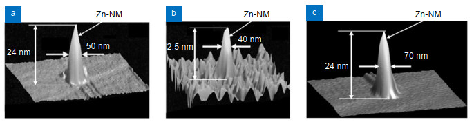
Zn(C2H5)2 ("DEZn" for short) was adopted as a specimen molecule. A DP was created on the tip of the fiber probe by irradiating the end of the fiber probe with light. Gaseous DEZn molecules, filled in a vacuum chamber, dissociated when these molecules jumped into the DP field. Here, the tip of the fiber probe and the molecule correspond to NM1 and NM2, respectively. The dissociated Zn atom subsequently landed on the substrate. After a short migration on the substrate, the Zn atom was adsorbed on the substrate. By repeating these dissociation and deposition processes, the number of adsorbed Zn atoms increased, resulting in the deposition of Zn atoms and the formation of a nanometer-sized metallic Zn-NM on the substrate.
For comparison, in the case of dissociating the DEZn molecules by using conventional propagating light, the wavelength was required to be shorter than 270 nm (photon energy 4.59 eV) for exciting an electron in the DEZn molecule (refer to the common view [c]). By noting this requirement, the following ingenious contrivances (ⅰ)-(ⅲ) were employed in order to confirm that the DEZn molecules were dissociated only by the DP in the PCVD above.
(ⅰ) The wavelength of the propagating light for creating the DP was set longer than 270 nm, contrary to the common view [c]. As a result, it was expected that the DEZn molecules would not be dissociated even if they were irradiated with the propagating light that leaked out from the tip of the fiber probe into the vacuum. Instead, it was expected that the DEZn molecules would be dissociated only by the DP on the tip due to the following phenomenon: [
(ⅱ) In order to insure that the contribution of the propagating light was excluded (refer to (ⅰ)), an unreliable fiber probe was used to intentionally cause the propagating light to leak out from the taper and tip of the fiber probe into the vacuum. That is, the fiber probe used here was fabricated by heating and mechanically pulling the fiber to form a sharp tip. This was a very primitive method in comparison with the high-precision and highly reproducible selective etching method
(ⅲ) For further insurance, the DEZn molecules were replaced by zinc-bis(acetylacetonate) ("Zn(acac)2" for short) molecules
![]()
Figure 1.Shear-force microscopic images of Zn-NMs formed on a sapphire substrate.Dissociated molecules are DEZn ((
It should be pointed out that the maximum size aDP, Max of the DP was estimated from the experimental results of the PCVD above
![]()
Figure 2.Dependence of the deposition rate
It should be noted that the FWHM values in
By using the nano-fabrication technology above, a variety of two-dimensional patterns have been formed by scanning a fiber probe, like a picture drawn with a single stroke of the pen
2) Technology not using a fiber probe or an aperture
This part reviews a novel autonomous nano-fabrication technology that requires neither fiber probes nor apertures, resulting in drastic increases in the working efficiency. A representative example is autonomous smoothing of a material surface: The material to be smoothed is installed in a vacuum chamber, and the chamber is also filled with gaseous molecules. By irradiating the material surface with light, the DP is created at the tips of the bumps on the rough material surface. That is, the bumps play the role of a fiber probe for creating the DP. If the molecules jump into the DP field, they are dissociated, as was the case of the PCVD in 1). The chemically active atoms, created as a result of this dissociation, selectively etch the tips of the bumps away, while the flat part of the surface remains unetched. The etching autonomously starts by light irradiation and the surface roughness decreases gradually as etching progresses. The etching autonomously stops when the bumps are annihilated and the DP is not created anymore.
The disc surface of a synthetic silica substrate (30 mm diameter) was etched by using gaseous Cl2 molecules. Although light with a wavelength shorter than 400 nm was required for conventional photo-dissociation (common view [c]), the present method used visible light with a wavelength of 532 nm based on Phenomenon 8. Etching by active Cl atoms decreased the surface roughness to as low as 0.13 nm. A laser mirror was produced by coating a high-reflection film on the smoothed substrate surface, and its damage threshold to the high-power ultraviolet laser light pulses was evaluated. The threshold value was confirmed to be as high as twice that of the commercially available strongest mirror whose substrate surface was polished by a conventional chemical-mechanical polishing technology
Gaseous O2 molecules can be also used for autonomous etching because the O atoms created by the dissociation are chemically active. The advantage is that etching can be carried out in atmospheric conditions by using O2 molecules in air, and thus, a vacuum chamber is not required.
![]()
Figure 3.The ratio of the standard deviation of the roughness of the PMMA surface before and after etching.(
In
![]()
Figure 4.Light emission spectra of the Si-LED.The substrate temperature and the injection current were 283 K and 2.45 A, respectively. Downward arrows A–D represent the spectral peaks at
Since the DPs are always created on the tip of the bump on the material surface under light irradiation, the present autonomous etching has been applied to a variety of surface profiles. These included a convex surface, a concave surface, and the inner surface of a cylinder. As an example, this etching has smoothed the side surface of a diffraction grating composed of parallel linear corrugated patterns
Energy conversion
Since the DP field has a broad spectrum, the novel phenomena of energy up- and down-conversion are expected. Three kinds of such energy conversions are reviewed in this section.
1) Conversion from optical to optical energy
Energy up-conversion, i.e., the conversion from infrared to visible light, has been realized. In this process, phonons in the DP provided their energies to the electrons in NMs. NMs of DCM, coumarine 540A, and stilbene 420 dye molecules were used as specimens for demonstrating the up-conversion. By irradiating them with infrared light of 0.8–1.3 μm wavelength, the DP created on one NM was transferred to the adjacent NMs. These NMs received the DP energy that contained the phonon energy, and thus, they respectively emitted red, green, and blue light
Energy down-conversion has also been realized by using an autonomously grown optically curable resin
As an application of this down-conversion, a novel plastic film was fabricated by dispersing ZnO and DCM NMs into it
2) Conversion from optical to electrical energy
Novel devices for optical to electrical energy conversion that exhibited the energy up-conversion feature originating from the DP have been fabricated. One example is a photovoltaic device using an organic thin film of P3HT. By depositing Ag nanoparticles on the device surface using a novel DP-assisted rf-sputtering method, the conformation of the electrode surface was autonomously controlled
3) Conversion from electrical to optical energy
This part reviews Si light-emitting diodes (LEDs), Si lasers, and SiC polarization rotators as examples of the conversion from electrical to optical energy. Phenomena contrary to the common view [e] are also demonstrated.
Crystalline Si has long been a key material supporting the development of modern technology for more than half a century because of its numerous advantages, such as Si's abundance in the earth's crust, and its widespread use for electronics. However, because Si is an indirect- transition-type semiconductor, it has been considered to be unsuitable for light-emitting devices: Since the bottom of the conduction band and the top of the valence band in Si are at different positions in reciprocal lattice space, the momentum conservation law requires an interaction between an electron–hole pair and phonons for radiative recombination. However, the probability of this interaction is very low.
Nevertheless, Si has been the subject of extensive study for the fabrication of light-emitting devices. These include studies using porous Si
The problems above have been solved by using the DP because the phonons in the DP can provide momenta to the electron to satisfy the momentum conservation law
① Infrared Si-LEDs
Fabrication and operation methods are reviewed here by taking an infrared Si-LED as a first example. An n-type Si substrate was used, in which as atoms or Sb atoms were doped. As the first step, the substrate surface was transformed to a p-type material by implanting B atoms, forming a p-n homojunction. Metallic films were coated on the substrate surfaces to serve as electrodes.
As the next step, this substrate was processed by a novel fabrication method named DP-assisted annealing: By current injection, Joule heat was generated, which caused the B atoms to diffuse. During this Joule-annealing, the substrate surface was irradiated with infrared light (for example, 1.342 μm-wavelength light). Because its photon energy hνanneal (=0.925 eV) was sufficiently lower than the bandgap energy Eg (=1.12 eV) of Si, the light could penetrate into the Si substrate without suffering absorption. Then, the light reached the p-n homojunction to create the DP on the B atom. The created DP localized at this impurity B atom, which manifested the following phenomenon: [
The phonons in the created DP can provide momenta to the electron nearby to satisfy the momentum conservation law, resulting in radiative recombination for photon emission. This is stimulated emission triggered by the irradiated infrared light. The emitted light propagated out from the crystal to the outside, which indicated that part of the Joule energy used for diffusing the B atoms was dissipated in the form of optical energy, resulting in local cooling that locally decreased the diffusion rate. As a result, by the balance between heating by the Joule energy and cooling by the stimulated emission, the spatial distribution of B atoms varied and reached a stationary state autonomously. This stationary state was expected to be the optimum for efficient creation of the DPs and for efficient LED operation because the probability of spontaneous emission was proportional to that of the stimulated emission described above.
The optimum condition for the DP-assisted annealing has been found based on a two-level system model. That is, the optimum ratio between the irradiated photon number and the injected electron number per unit time was 1:1
The device fabricated above was operated as an LED by simple current injection, similar to the case of operating conventional LEDs. By injecting a current of 3.0 A into a device with an areal size of 0.35 mm×0.35 mm, a CW output optical power as high as 2.0 W was obtained at a substrate temperature of 77 K. A power as high as 200 mW was obtained even at room temperature (283 K)
It should be noted that the photon energy emitted from the conventional LEDs was governed by Eg. However, in the present Si-LED, the energy difference between hνanneal and Eg was compensated by the created phonon energy. The origin of this compensation was attributed to the spatial distribution of B atoms that was autonomously controlled during the DP-assisted annealing. For this control, the irradiated light served as a source for creating the DP during the DP-assisted annealing. It has been theoretically confirmed that the DP, after being created and localized on the B atom (Phenomenon 10), coupled more efficiently with localized phonons than with non-localized ones. It has been also confirmed that a B atom-pair served as a resonant cavity to confine and localize phonons, resulting in localized phonon creation
For comparing these theoretical confirmations with experimental results, the three-dimensional spatial distribution of B atoms at the p-n homojunction was acquired by atom probe field ion microscopy of sub-nanometer spatial resolution. By analyzing the acquired data, it was found that the B atoms were apt to form pairs with a length d=3a (a (=0.54 nm) is the lattice constant of the Si crystal), and the formed pairs were apt to orient along a plane parallel to the top surface of the Si crystal
It should be noted that the Si crystal is composed of multiple cubic lattices, and the value of the required phonon momentum has to be h/a for the radiative recombination of the electron (at the bottom of the conduction band at the X-point in reciprocal space) and the positive hole (at the top of the valence band at the Γ-point) to take place. It should be also noted that the value of the phonon momentum is h/3a when the phonon localizes at the B atom-pair with d=3a. By comparing these values of momenta, it is found that the DP created and localized at this B atom-pair provides three phonons for recombination. As a result, the emitted photon energy hνem is expressed as hνem= Eg–3Ephonon. By substituting the values of Eg (= 1.12 eV) and the relevant optical mode phonon energy Ephonon (=65 meV) into this equation, the value of hνem is derived to be 0.93 eV, which is nearly equal to the photon energy hνanneal (=0.95 eV) irradiated during the DP-assisted annealing. This numerical relation is consistent with the spectral feature in
The peaks B and C in this figure are the second and third harmonics of the phonon contributions, respectively. PB was observed also with respect to the photon spin. That is, the polarization direction of the emitted light was identical to that of the light irradiated during the DP-assisted annealing
② Visible LEDs
The second example is visible LEDs fabricated by using crystalline Si and that exhibit the PB phenomenon. Specifically, blue, green, and red light-emitting LEDs were fabricated by radiating blue, green, and red light, respectively, during the DP-assisted annealing
A variety of visible LEDs have been developed by using crystalline SiC even though it is also a well-known indirect transition-type semiconductor. They were fabricated by irradiating them with UV-violet, bluish-white, blue, and green light during the DP-assisted annealing. The fabricated devices emitted UV-violet, bluish-white, blue, and green light, respectively
③ Infrared Si-lasers
The third example is high-power infrared Si-lasers. A simple ridge waveguide (10 μm-width and 2 μm-height) was built-in, and the cleaved facets were used as mirrors of a Fabry-Perot cavity (550 μm-cavity length)
![]()
Figure 5.Light emission spectra and output optical power of Si lasers.(
By modifying the device structure above, high-power infrared laser devices were fabricated. The ridge waveguide was not built into them because further increases in the optical confinement efficiency were not expected in this waveguide as long as the device had a p-n homojunction. Instead, the cavity length was increased to 15 mm to realize high-power lasing by utilizing the very low infrared absorption of crystalline Si.
④ Polarization rotators
The last example is polarization rotators fabricated by using a SiC crystal. The fabrication method was equivalent to that of the visible SiC-LEDs of the second example: By implanting Al atoms into an n-type SiC substrate, the substrate surface was transformed to a p-type material, forming a p-n homojunction. By the DP-assisted annealing, during which the substrate surface was irradiated with the 405 nm-wavelength light, diffusion of Al atoms was autonomously controlled to realize the optimum spatial distribution of Al atoms for light emission. As a result, the device worked as a visible LED.
In order to use it as a polarization rotator, an H-shaped electrode was installed on the top surface. By current injection to this electrode, electrons were injected into the p-n homojunction and a magnetic field was generated. It is expected that this current injection rotated the polarization of the light incident into the device. Linearly polarized 405 nm-wavelength light was made normally incident on the top surface of this device. This was because, due to PB, it was also expected that the rotation angle was the largest when its wavelength was identical to that of the light irradiated during the DP-assisted annealing.
Meeting the expectations above, the polarization angle of the incident light actually rotated after propagating through the device. The Verdet constant was evaluated to be 660 deg/A from the measured values of the polarization rotation angle. This is 105–106 times those of conventional paramagnetic materials that are transparent in the visible region. The Faraday rotation angle was also as large as 2480 deg/cm. These large values demonstrated that the present SiC crystal exhibited a gigantic magneto-optical effect. Furthermore, the remanent magnetization was 0.36 mT, which corresponded to those in conventional ferromagnetic materials
In order to find the origin of such novel ferromagnetic properties, a magnetization curve was acquired at 27 ℃. Closed squares in
![]()
Figure 6.Magnetization curve for the SiC crystals, measured at 27 ℃.Closed squares and open circles are the results acquired after and before the DP-assisted annealing, respectively. They are fitted by the curves A and B, respectively.
The origin of this behavior has been attributed to the Al atom-pairs that were autonomously formed as a result of the DP-assisted annealing. That is, the ferromagnetic characteristic likely originated from the two electrons with parallel spins in the triplet state of the electron orbital in an Al atom-pair, which was more stable than the singlet state.
At the end of this part it should be pointed out that similar polarization rotators have also been fabricated by using ZnO crystals based on the same principle as in the SiC crystals above
Future directions
The studies reviewed in this paper identified the DP as a quantum field that is created as a result of the light-matter interaction in a nanometer-sized space. However, they also presented at least two theoretical difficulties. One was that the mode of the electromagnetic field could not be defined. The other was that the description of the spatial localization of the DP required the surrounding macroscopic subsystem to have a parabolic dispersion relation. As an urgent solution to overcome these difficulties, the theoretical methods in on-shell science were modified and applied to tentatively describe the physical nature of the DP.
Although the theoretical studies above were at a standstill, experimental studies have found the novel Phenomena 1–15. It should be noted that they cannot be described by conventional optical theories. This is because these theories treat only photons in a vacuum (free photons) and in a macroscopic material, whose dispersion relation is given by the mass-shell ("on-shell" for short). It has been popularly known that massless particles with non-zero spin, such as free photons, cannot be localized in space in the sense that the position operator cannot be defined
For a theoretical definition of the DP and for describing the Phenomena 1–15 above, the "off-shell" nature of the interaction has to be considered. That is, the DP is an off-shell quantum field that conspicuously deviates from the mass-shell. As has been well known, quantum field theories cannot be formulated without off-shell entities. In other words, the traditional particle description has failed to treat the quantum field of a composite system. Hence, DPs must be entities that are very different from Einstein's quanta of light or free photons.
Here, a fundamental question arises: How can the DP be described as an individual entity? As long as one sticks to the notion of individual entities as irreducible on-shell particles, it is impossible to treat the DP as an individual entity. However, a more general perspective, advocated by Ojima
By following this perspective, a basic idea can be proposed: In the interaction between light and NMs, certain families of modes of the composite system will behave as individuals. This behavior suggests that the DP is the quantum field of a composite system in which an electromagnetic field and an electron (or an exciton) interact in a nanometer-sized space. Furthermore, it is a virtual field localized in the nanometer-sized space within a short time duration. Thus, the DP is a quantum field whose nature is contrary to that of an on-shell photon. This means that conventional optical theories are incapable of giving a systematic description of Phenomena 1–15. Fortunately, however, several hints have been given to construct novel theories for describing the phenomena above by noting that the virtual photon plays an essential role in the electromagnetic Coulomb interactions. They are:
[A] The longitudinal mode of an electromagnetic field (the longitudinal wave) contributes to the Coulomb interaction
[B] The field interaction accompanies the 4-momentum
[C] Although the spacelike field is not spatially localized because it behaves as a stable wave, it becomes unstable and can localize if it interacts with a timelike field
By referring to these hints, novel theoretical studies have commenced by relying on physical bases
Furthermore, mathematics-based theoretical studies are in progress that will serve as invaluable guides for gaining a deep understanding of the concepts of the physics-based theories for the phenomena that originate from the DP
One of the promising future direction of DP science is to propel the theoretical studies above in collaboration with experimental ones. By using the fruits of these studies, further developments of application technologies are expected, resulting in further disruptive innovations.
Summary
This paper reviewed the progress in optical sciences dealing with the ONF. After the introduction, it pointed out that the ONF was an electromagnetic field that is created and localized in an NM, or on its surface, under light illumination.
Next, it reviewed the classical studies of the ONF that explored the possibilities of creating and using the ONF. It described that the studies on the ONF, called the near field optics, started for realizing disruptive innovation by breaking through the diffraction limit of optical microscopy. Its methodology was proposed in the 1920s to 1950s, and experimental demonstrations were carried out in the 1980s and 1990s. It was pointed out that the classical studies of the ONF had already come to an end without answering the essential questions on the origin of the near-field optical interaction.
However, even after this end, basic studies on the ONF were steadily continued by a small number of scientists. These included studies on the concepts and principles of the ONF, with the aim of answering the questions above. As a result, the ONF was identified as an off-shell quantum field, i.e., a virtual field localized in a nanometer-sized space within a short time duration. Based on this identification, a novel off-shell science has started by noting that the dispersion relation between the energy and momentum was invalid for the ONF. This quantum field is now called the DP because it is created as a result of the interaction between photons and electrons (or excitons) in a NM, and thus, it accompanies the energies of electrons or excitons. In the other words, the DP is a quantum field created in a system composed of electromagnetic fields and NMs.
Novel Phenomena 1–15 were reviewed that have been found in a series of experimental studies on the DP. Phenomena 1–5 are general in concepts. Phenomena 6–7 are observed in novel photonic devices and in information processing, and 8–9 are in nano-fabrication. Phenomena 10–15 correspond to novel observations in energy conversion of light emitting semiconductors by utilizing DP. They are contrary to the common views that have been accepted for a long time by conventional optical science. By applying these phenomena, a variety of technologies have been developed. These include nanometer-sized optical devices (including their applications to information transmission and processing systems), nano-fabrication technology (photochemical vapor deposition, lithography, and smoothing of material surfaces), and three kinds of energy conversion technologies. Among these energy conversion technologies, the electrical to optical energy conversion used a DP that was created as a result of electrical excitation by current injection. This conversion realized high-power light emitting diodes and lasers by using crystalline Si, which is a typical indirect-transition-type semiconductor. A polarization rotator was realized by using crystalline SiC (also an indirect-transition-type semiconductor) that exhibited a gigantic magneto-optical effect.
Finally, the advent of novel theories was reviewed. These included a theory using electromagnetic response functions, a theory based on spatio-temporal vortex hydrodynamics supported by relativity theory, quantum probability theory, quantum measurement theory, and a theory based on micro–macro duality.
Competing interests
The author declares no competing financial interests.
References
[1] Ohtsu M.Near-Field Nano/Atom Optics and Technology(Springer, Berlin, 1998).
[2] Zhu X, Ohtsu M.Near-Field Optics: Principles and Applications(World Scientific, Singapore, 2000).
[3] M Ohtsu. From classical to modern near-field optics and the future. Opt Rev, 21, 905-910(2014).
[5] J A O'Keefe. Resolving power of visible light. J Opt Soc Am, 46, 359(1956).
[6] H A Bethe. Theory of diffraction by small holes. Phys Rev, 66, 163-182(1944).
[7] C J Bouwkamp. On the diffraction of electromagnetic waves by small circular disks and holes. Philips Res Rep, 5, 401-422(1950).
[8] E A Ash, G Nicholls. Super-resolution aperture scanning microscope. Nature, 237, 510-512(1972).
[9] Pohl D W, Courjon D.Near Field Optics (Kluwer, Dordrecht, 1993).
[14] Mononobe S, Saiki T.Chs 3 and 4 in Near-Field Nano/Atom Optics and Technol .(ed Ohtsu M.Springer Tokyo, 1998).
[17] L Malmqvist, H M Hertz. Trapped particle optical microscopy. Opt Commun, 94, 19-24(1992).
[20] J M Guerra. Photon tunneling microscopy. Appl Opt, 29, 3741-3752(1990).
[22] X S Xie, R C Dunn. Probing single molecule dynamics. Science, 265, 361-364(1994).
[30] Eah S K, Jhe W, Saiki T, Ohtsu M.Study of quantum optical effects with scanning near-field optical microscopy In Proceedings of theFirstAsia-PacificWorkshoponNearFieldOptics(1996).
[35] Ohtsu M.Handbook of Nano-Optics and Nanophotonics (Springer, Heidelberg, New York, 2013).
[36] Ohtsu M, Yatsui T.Progress in Nanophotonics 4(Springer, Heidelberg, 2017).
[52] http://doi.org/10.14939/1802R.001.v1.
[54] Kobayashi K, Sangu S, Ohtsu M, Ch 5 in Progress in Nano-Electro-Optics(Springer, Heidelberg, 2003).
[60] Koike M, Miyauchi S, Sano K, Imazono T.Ch.9 in Nanophotonics and Nanofabrication.(ed Ohtsu M.Wiley-VCH, 2009).
[62] T Yatsui, W Nomura, M Ohtsu. Realization of ultraflat plastic film using dressed-photon-phonon-assisted selective etching of nanoscale structures. Adv Opt Technol, 2015, 701802(2015).
[63] D W Allan. Statistics of atomic frequency standards. Proc IEEE, 54, 221-230(1966).
[73] Yatsui T.Progress in Nanophotonics 5(Springer, 2018).
[88] Ohtsu M.Silicon Light-Emitting Diodes and Lasers(Springer, Heidelberg, 2016).
[90] Kawazoe T.High power Silicon laser based on the dressed photon technology.In Proceedings of 2017 International Conference on Solid State Devices and Materials 413-414(2017).
[91] Ohtsu M, Ojima I, Sakuma H.Ch 1, Vol 62 in Progress in Optics(ed Visser T.Elsevier, 2019)
[92] Ohtsu M.Ch 6 and Ch 8 in Silicon Light-Emitting Diodes and Lasers(Springer, Heidelberg, 2016).
[95] Ojima I.Micro-macro duality in quantum physics.Ch 12 in Stochastic Analysis: Classical and Quantum-Perspectives of White Noise Theory(ed T Hida.World Scientific, 2005).
[96] Ojima I.Nakanishi-Lautrup, B-field, crossed product and duality.In ResearchonQuantumFieldTheory, RIMSWorkshop(2006).
[97] G F Dell'Antonio. Support of a field in p space. J Math Phys, 2, 759-766(1961).
[99] Yatsui T.Vol 5 in Progress in Nanophotonics(Springer, 2018). [100.Ohtsu M, Ojima I, Sakuma H.Ch 2, Vol 64 in Progress in Optics(ed Visser T D.Elsevier, 2019).
[100] Ohtsu M, Ojima I, Sakuma H. Ch 2, Vol 64 in Progress in Optics (ed Visser T D. Elsevier, 2019).


Set citation alerts for the article
Please enter your email address

© Copyright 2018-2021 | Chinese Laser Press. All Rights Reserved 沪ICP备15018463号-20