
Motoichi Ohtsu. History, current developments, and future directions of near-field optical science[J]. Opto-Electronic Advances, 2020, 3(3): 190046-1
- Opto-Electronic Advances
- Vol. 3, Issue 3, 190046-1 (2020)
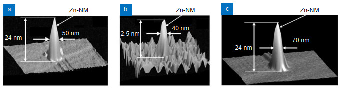
Fig. 1. Shear-force microscopic images of Zn-NMs formed on a sapphire substrate.Dissociated molecules are DEZn ((a ) and (b )) and Zn(acac)2 (c ). The wavelengths of the propagating light for creating the DP were 488 nm (a), 684 nm (b), and 457 nm (c).
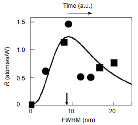
Fig. 2. Dependence of the deposition rate R (atoms/s/W) on the FWHM of the Zn-NM.FWHM increased with increasing deposition time. The number of atoms deposited per unit time was normalized to the irradiated light power (W ) to derive the rate R . The wavelength of the propagating light for creating the DP was 325 nm. Closed circles and squares represent the measured values when the powers of the light incident to the fiber probe were 5 μW and 10 μW, respectively. The downward arrow represents the value of 2a p.
Fig. 3. The ratio of the standard deviation of the roughness of the PMMA surface before and after etching.(a ) and (b ) are the results acquired by illuminating the surface with light having wavelengths of 325 nm and 213 nm, respectively. The downward arrows represent the values of l that are equal to the wavelengths above.
Fig. 4. Light emission spectra of the Si-LED.The substrate temperature and the injection current were 283 K and 2.45 A, respectively. Downward arrows A–D represent the spectral peaks at E g–3E phonon, E g–6E phonon, E g–9E phonon, and E g, respectively.
Fig. 5. Light emission spectra and output optical power of Si lasers.(a ), (b ) Spectral profiles above and below the threshold, respectively, of a 550 μm-length device with a ridge waveguide. The threshold current density was 1.1 A/cm2 under CW operation at room temperature (25 ℃). (c ), (d ) Relation between the injected current density and the output optical powers of 15 mm-long and 30 mm-long devices, respectively. J th is the threshold current density. Closed circles in (d) are a copy of those in (c).
Fig. 6. Magnetization curve for the SiC crystals, measured at 27 ℃.Closed squares and open circles are the results acquired after and before the DP-assisted annealing, respectively. They are fitted by the curves A and B, respectively.

Set citation alerts for the article
Please enter your email address
© Copyright 2018-2021 | Chinese Laser Press. All Rights Reserved 沪ICP备15018463号-20