
Yonggang Gu, Jian Niu, Jian Yang, Fang Dong, Hongxing Xu. [J]. Laser & Optoelectronics Progress, 2023, 60(7): 0714005
- Laser & Optoelectronics Progress
- Vol. 60, Issue 7, 0714005 (2023)
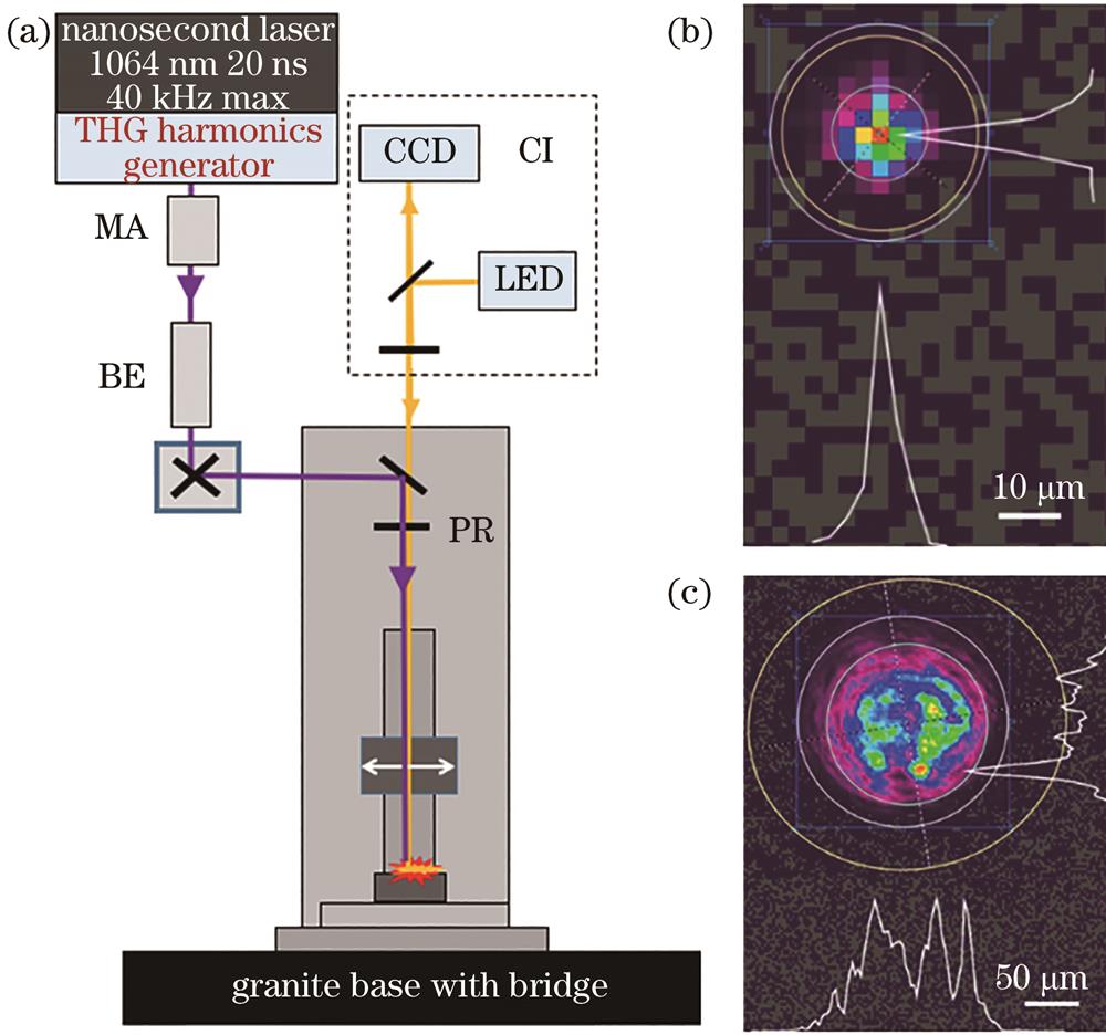
Fig. 1. Laser processing setup. (a) Schematic of the laser processing setup; (b) laser intensity distribution at the focal plane; (c) laser intensity distribution at the sample surface
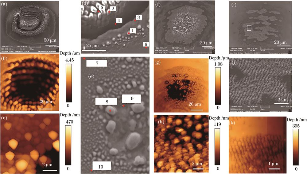
Fig. 2. SEM and AFM images of the micro-nano structures formed on GaN thin films using single 355 nm nanosecond pulses. (a)-(c) Structures induced by a 2.44 mJ laser pulse; (d)(e) locations in (a) where the elemental analyses were performed; (f)-(h) structures induced by a 0.67 mJ laser pulse; (i)-(k) structures induced by a 0.25 mJ laser pulse
Fig. 3. SEM images of the micro-nano structures formed on GaN thin films by 400 ns laser pulses. (a) Overall view of induced surface patterns; (b) enlarged views showing alternate concentric stripes on the thin film surface; (c) element weight percentages in adjacent stripes
Fig. 4. Effect of laser polarization direction (laser polarization angle is rotated by 30° between adjacent sets of experiments, and yellow arrows indicate the incident laser polarization directions)
Fig. 5. Surface micro-nano structures induced by circularly polarized laser pulses

Set citation alerts for the article
Please enter your email address
© Copyright 2018-2021 | Chinese Laser Press. All Rights Reserved 沪ICP备15018463号-20