Author Affiliations
1School of Physics and Technology, Wuhan University, Wuhan 430072, Hubei , China2State Key Laboratory of Precision Spectroscopy, East China Normal University, Shanghai 200062, China3The Institute of Technological Sciences, Wuhan University, Wuhan 430072, Hubei , Chinashow less
Abstract
Gallium nitride (GaN) has widespread applications in the semiconductor industry because of its desirable optoelectronic properties. The fabrication of surface structures on GaN thin films can effectively modify their optical and electrical properties, providing additional degrees of freedom for controlling GaN-based devices. Compared with lithography-based techniques, laser processing is maskless and much more efficient. This paper shows how surface micro-nano structures can be produced on GaN thin films using 355 nm nanosecond laser irradiation. The effects of the laser pulse energy, number of pulses, and polarization direction were studied. It was found that distinct micro-nano structures were formed under different irradiation conditions, and their geometries and elemental compositions were analyzed. The results indicate that different types of surface micro-nano structures can be produced on GaN thin films in a controllable manner using 355 nm nanosecond laser irradiation. The results of our study provide valuable guidance for the surface modification of GaN-based optoelectronic devices.1 Introduction
Gallium nitride(GaN)is a very important direct wide bandgap semiconductor material that is widely used in optoelectronic and power electronic devices[1-4]. One particular advantage of the material is the ability to tune its bandgap by appropriately replacing some of the gallium with aluminum and forming AlxGa1-xN. This provides bandgaps ranging from 3.4 eV(GaN)to 6.1 eV(AlN)[5-6],enabling the fabrication of deep ultraviolet light emitting diodes(DUV-LEDs)and laser diodes(LDs)for applications in bio-chemical detection[7-9],medical diagnostics[10],and free-space communication[11-12]. In addition to tuning its chemical composition,surface texturing through the formation of surface micro-nano structures has recently emerged as an alternative method for actively manipulating the optical and electrical properties of GaN[13-15]. For example,GaN-based LEDs,which are widely used in many applications,make use of the quantum-confined Stark effect through the quantum nanostructures formed on their surfaces. These structures are usually formed by a combination of inductively coupled plasma reactive ion etching and nanoparticle lithography. However,this complex processing technique not only reduces production efficiency but also poses a great challenge to device quality control[16]. Thus,new methods of fabricating surface micro-nano structures on GaN thin films are in demand to improve the properties of GaN devices.
As an improvement over conventional,complex,and time-consuming lithography-based surface texturing techniques,laser processing is maskless and efficient,representing a promising alternative strategy[17-22]. For example,the formation of laser-induced periodic surface structures(LIPSS)has attracted the attention of the scientific community since its discovery[23-24]. LIPSS have been reported in metals[25-26],semiconductors[27-28],dielectrics[29-30],and polymer films[31-32]. The mechanism of LIPSS formation has been studied theoretically as well as through ultrafast experimental observations[33-35]. Moreover,the size,shape,and orientation of LIPSS can be controlled by exploiting the self-interference and self-organization of the material by tuning laser irradiation parameters such as the fluence,wavelength,pulse number,and polarization[36-41]. The formation of LIPSS has been utilized to generate superhydrophobic,anti-reflective,colored,and drag-resistant surfaces by mimicking numerous biological features such as those of lotus leaves and moth eyes[42]. Understanding the formation of laser-induced micro-nano structures on GaN can provide an important foundation for the active tuning of GaN device properties.
In this study,surface micro-nano structures were produced on GaN thin films using 355 nm nanosecond laser irradiation. Under different laser irradiation conditions,distinct patterns could be formed,including craters containing hillocks,randomly distributed nanoparticles,LIPSS,and alternate concentric stripes. The geometries and elemental compositions of these surface structures were analyzed in detail. The results of this study demonstrate the possibility of controlling the formation of micro-nano structures on GaN thin films,which provides an important physical foundation for the development of processing techniques for GaN-based optoelectronic devices.
2 Experimental setup
2.1 Preparation of GaN films
The GaN thin films(3 µm thick)used in the experiment were grown on the c-planes of sapphire substrates(440 µm thick)using metal organic chemical vapor deposition(MOCVD). The MOCVD was performed in a multi-wafer rotating disk reactor at 1040 ℃,with GaN buffer layers(20 nm thick)grown at 530 ℃.
2.2 Laser processing setup
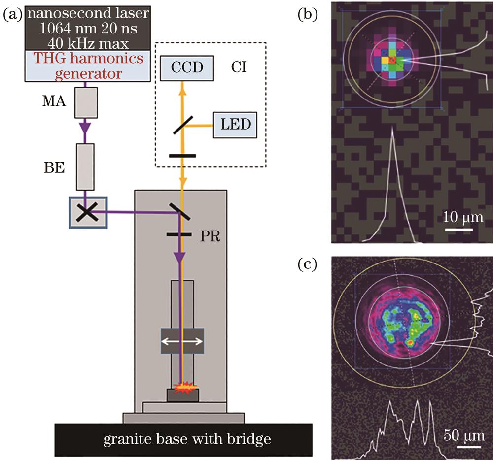
A schematic of the laser processing setup is given in Fig. 1(a). The laser processing experiment was performed with a nanosecond laser system(Wuhan Huari). The laser system emitted linearly polarized laser pulses with a wavelength of 1064 nm and a pulse width of 20 ns. The maximum repetition rate was 40 kHz,and the maximum average output power was 15 W. The laser pulses first passed through a third-harmonic generation(THG)harmonics generator,and 355 nm UV pulses were generated. These passed through a motorized attenuator(MA),beam expander(BE),and polarization rotator(PR)into a galvo scanner. At the exit of the scanner,a plano-convex lens with a focal length of 50 mm focused the laser to a spot size of 10 µm,with the intensity distribution shown in Fig. 1(b). The sample surface deviated from the focal plane by 2 mm,where the laser spot size was 150 µm,with the intensity distribution shown in Fig. 1(c). The laser pulse energy at the sample surface could be adjusted by tuning the pump current or MA,while the polarization direction could be controlled by the PR. The samples were mounted on a three-axis positioning system(Aerotech). A coaxial imaging(CI)system composed of a charge coupled device(CCD)and an LED was used to monitor the sample in real time.

Figure 1.Laser processing setup. (a) Schematic of the laser processing setup; (b) laser intensity distribution at the focal plane; (c) laser intensity distribution at the sample surface
2.3 Characterization
After laser processing,the surface morphology of each sample was analyzed using an emission scanning electron microscope(SEM,MIRA 3 LMH)and atomic force microscope(AFM,Veeco Nanoscope IIIa). An elemental analysis was performed by SEM-electron energy disperse spectroscopy(SEM-EDS,Aztec Energy X-Max 20).
3 Results and discussions
3.1 Single-pulse irradiation
Figs. 2(a)-(c)show SEM and AFM images of the micro-nano structures formed on a GaN thin film after a single pulse of laser irradiation with a pulse energy of 2.44 mJ. The elemental compositions at various locations within the structures[Figs. 2(d)and(e)]were determined using SEM-EDS and are listed in Table 1. Fig. 2(a)shows an SEM image of the sample surface after using a laser pulse energy of 2.44 mJ. A crater formed at the center,with regularly distributed hillocks inside of it. Fig. 2(b)shows the corresponding AFM image,indicating a top-to-bottom height of 4.45 µm,which is larger than the thickness of the original GaN thin film. Fig. 2(c)shows an enlarged image of the white square region in Fig. 2(a),where some hexagonal grains can be observed.
Figure 2.SEM and AFM images of the micro-nano structures formed on GaN thin films using single 355 nm nanosecond pulses. (a)-(c) Structures induced by a 2.44 mJ laser pulse; (d)(e) locations in (a) where the elemental analyses were performed; (f)-(h) structures induced by a 0.67 mJ laser pulse; (i)-(k) structures induced by a 0.25 mJ laser pulse
Fig. 2(d)shows the locations where the SEM-EDS measurements were performed(Table 1). At locations 2,4,and 5,only oxygen and aluminum were detected,indicating that the GaN thin film was completely ablated away,leaving the bare sapphire substrate. At location 3,gallium and nitride were primarily detected,indicating that GaN was still present. At locations 1 and 6,complex mixtures of different elements were observed. It is known that GaN begins to decompose at 1050 ℃ through the following reaction:2GaN(s)= 2Ga(g)+ N2(g). The gaseous gallium easily oxidizes and forms Ga2O3 under ambient conditions. This oxidation reaction renders the laser processing of GaN more complicated compared to other semiconductor materials such as silicon. Moreover,GaN melts at approximately 1700 ℃. Therefore,Ga2O3 and liquid GaN droplets can easily form during laser irradiation as a result of thermal effects.
When the pulse energy was tuned down to 0.67 mJ,as shown in the SEM and AFM images in Figs. 2(f)-(h),a crater formed at the center and LIPSS could be observed at the periphery. The central crater was shallower than that formed when using the higher pulse energy,and the GaN film was not completely ablated away. Elemental analysis indicated the presence of both Ga2O3 and GaN nanoparticles randomly distributed on the thin film surface.
Finally,when the pulse energy was further reduced to 0.25 mJ,LIPSS formed on the GaN surface[Figs. 2(i)-(k)]. The period of the stripes in the pattern was close to a wavelength of 355 nm,corresponding to low spatial frequency LIPSS(LSFL). Some embedded particles could be observed within the LSFL. The top-to-bottom height of the LIPSS was approximately 400 nm,which was much shallower than the thin film thickness.
The experimental results show different regimes after the single-pulse processing of GaN thin films. At a high laser pulse energy,most of the GaN material is ablated away,leaving a deep crater containing randomly distributed hillocks. Ga2O3 or GaN nanoparticles can be observed as a result of the thermal effects of the laser pulse irradiation. At a medium laser pulse energy,a shallow crater forms at the center,and LIPSS form at the periphery. At a low laser pulse energy,LIPSS form on the GaN surface with embedded nanoparticles. The spatial frequency of the LIPSS correspond to LSFL.
3.2 Multi-pulse irradiation
We used the low laser pulse energy corresponding to the LIPSS formation regime to study the effect of multi-pulse irradiation. Fig. 3(a)shows an SEM image of the surface patterns induced by multiple laser pulses. Note that each spot in Fig. 3(a)corresponds to one of the 400 laser pulses. An enlarged image[Fig. 3(b)]reveals that alternating concentric stripes with widths of approximately 10 μm formed on the GaN thin film surface. Two distinct patterns can be observed:randomly distributed large nanoparticles(cyan square)and LIPSS with embedded nanoparticles(gray square). The results of elemental analyses[Fig. 3(c)]indicate that the two patterns have different extents of oxidation. The region with large nanoparticles contains roughly 25% oxygen by weight. Thus,these nanoparticles could be either Ga2O3 or GaN. The region with LIPSS has barely any oxygen content. Thus,the embedded nanoparticles should be GaN.
Figure 3.SEM images of the micro-nano structures formed on GaN thin films by 400 ns laser pulses. (a) Overall view of induced surface patterns; (b) enlarged views showing alternate concentric stripes on the thin film surface; (c) element weight percentages in adjacent stripes
The differences in the oxidation and particle morphology indicate different temperatures on adjacent stripes. The regions with more oxidation experience a higher temperature during multi-pulse laser irradiation. It is possible that these alternate stripes are formed as a result of the alternate distribution of laser field energy during irradiation caused by some interference effects. The detailed reason deserves further investigation.
We only studied the formation of surface structures under a single pulse and 400 pulses. We selected N = 400 as the pulse number because clear and high-quality surface structures composed of alternate stripes form under 400 laser irradiation pulses. Future studies will consider the evolution of surface micro-nano structures with a gradual increase in the number of pulses.
3.3 Effect of laser polarization
Laser polarization is known to have a large influence on the formation of LIPSS. Thus,the polarization angle of the linearly polarized laser pulses was rotated,and we studied its effect on the LIPSS. Fig. 4 shows the results of six sets of experiments where we rotated the laser polarization angle by 30° between adjacent sets of experiments. The yellow arrows indicate the incident laser polarization directions. For each of them,the number of laser pulses is fixed at 400. As can be seen from Figs. 4(a1)and(f1),the alternate concentric stripes always form regardless of the polarization angle. However,the LIPSS direction changes along with the laser polarization angle[Figs. 4(a2)and(f2)]. The LIPSS direction is always perpendicular to the incident laser direction,in agreement with most LIPSS studies on metals and semiconductors.
Figure 4.Effect of laser polarization direction (laser polarization angle is rotated by 30° between adjacent sets of experiments, and yellow arrows indicate the incident laser polarization directions)
Finally,as illustrated by Fig. 5,circularly polarized laser pulses cause a considerable change in surface structure. Both the alternate stripes and LIPSS disappear,leaving only circularly distributed islands and numerous random nanoparticles. This clearly demonstrates that laser polarization has a crucial effect on the formation of LIPSS. Only linear polarization induces periodic structures.
Figure 5.Surface micro-nano structures induced by circularly polarized laser pulses
4 Conclusions
Surface micro-nano structures can be induced on GaN thin films by 355 nm nanosecond laser pulse irradiation. The effects of the laser pulse energy,number of pulses,and polarization direction on the surface structure formation were studied. For single-pulse irradiation,distinct patterns,including craters containing hillocks,randomly distributed nanoparticles,and LIPSS,can be formed under different laser pulse energies. For multi-pulse irradiation,alternate stripes appear with different extents of oxidation corresponding to distributed nanoparticles and LIPSS. The laser polarization was found to play an important role in LIPSS formation. The controllable formation of micro-nano structures by laser processing has potential applications in GaN-based optoelectronic devices.
References
[1] Rais-Zadeh M, Gokhale V J, Ansari A et al. Gallium nitride as an electromechanical material[J]. Journal of Microelectromechanical Systems, 23, 1252-1271(2014).
[2] Jayant Baliga B. Gallium nitride devices for power electronic applications[J]. Semiconductor Science and Technology, 28, 074011(2013).
[3] Chen K J, Häberlen O, Lidow A et al. GaN-on-Si power technology: devices and applications[J]. IEEE Transactions on Electron Devices, 64, 779-795(2017).
[4] Zhang B J, Liu Y. A review of GaN-based optoelectronic devices on silicon substrate[J]. Chinese Science Bulletin, 59, 1251-1275(2014).
[5] Liao Y T, Thomidis C, Kao C K et al. AlGaN based deep ultraviolet light emitting diodes with high internal quantum efficiency grown by molecular beam epitaxy[J]. Applied Physics Letters, 98, 081110(2011).
[6] Li D B, Jiang K, Sun X J et al. AlGaN photonics: recent advances in materials and ultraviolet devices[J]. Advances in Optics and Photonics, 10, 43(2018).
[7] Varghese A, Periasamy C, Bhargava L. Analytical modeling and simulation-based investigation of AlGaN/AlN/GaN bio-HEMT sensor for C-erbB-2 detection[J]. IEEE Sensors Journal, 18, 9595-9603(2018).
[8] Cimalla I, Will F, Tonisch K et al. AlGaN/GaN biosensor: effect of device processing steps on the surface properties and biocompatibility[J]. Sensors and Actuators B: Chemical, 123, 740-748(2007).
[9] Lee H H, Bae M, Jo S H et al. AlGaN/GaN high electron mobility transistor-based biosensor for the detection of C-reactive protein[J]. Sensors, 15, 18416-18426(2015).
[10] Pearton S J, Ren F. Gallium nitride-based gas, chemical and biomedical sensors[J]. IEEE Instrumentation & Measurement Magazine, 15, 16-21(2012).
[11] Wang W C, Wang H Y, Lin G R. Ultrahigh-speed violet laser diode based free-space optical communication beyond 25 Gbit/s[J]. Scientific Reports, 8, 1-7(2018).
[12] Rajbhandari S, McKendry J J D, Herrnsdorf J et al. A review of gallium nitride LEDs for multi-gigabit-per-second visible light data communications[J]. Semiconductor Science and Technology, 32, 023001(2017).
[13] Chang T L, Chen Z C, Lee Y C. Micro/nano structures induced by femtosecond laser to enhance light extraction of GaN-based LEDs[J]. Optics Express, 20, 15997-16002(2012).
[14] So H, Lim J, Senesky D G. Continuous V-grooved AlGaN/GaN surfaces for high-temperature ultraviolet photodetectors[J]. IEEE Sensors Journal, 16, 3633-3639(2016).
[15] Yang C C, Horng R H, Lee C E et al. Improvement in extraction efficiency of GaN-based light-emitting diodes with textured surface layer by natural lithography[J]. Japanese Journal of Applied Physics, 44, 2525(2005).
[16] Miyagawa R, Eryu O. Formation of femtosecond laser-induced periodic nanostructures on GaN[J]. Japanese Journal of Applied Physics, 58, SCCB01(2019).
[17] Nayak B K, Gupta M C. Self-organized micro/nano structures in metal surfaces by ultrafast laser irradiation[J]. Optics and Lasers in Engineering, 48, 940-949(2010).
[18] Boinovich L B, Emelyanenko A M, Modestov A D et al. Synergistic effect of superhydrophobicity and oxidized layers on corrosion resistance of aluminum alloy surface textured by nanosecond laser treatment[J]. ACS Applied Materials & Interfaces, 7, 19500-19508(2015).
[19] Cunha A, Elie A M, Plawinski L et al. Femtosecond laser surface texturing of titanium as a method to reduce the adhesion of Staphylococcus aureus and biofilm formation[J]. Applied Surface Science, 360, 485-493(2016).
[20] Cheng J H, Hu L X, Wang T J et al. Research progress of femtosecond laser-induced multifilament generation and regulation[J/OL]. Chinese Journal of Lasers, 1-29. http://kns.cnki.net/kcms/detail/31.1339.tn.20221028.1028.048.html
[21] Chen L, Wen G Q, Guo F et al. Fractal characteristics of microstructures on a superhydrophobic silicone rubber surface induced by a nanosecond laser[J]. Chinese Journal of Lasers, 48, 0602201(2021).
[22] Wang T Y, Bian J T, Li X et al. Effect of laser induced periodic surface structures on infrared emission characteristics of copper films[J]. Chinese Journal of Lasers, 48, 0401017(2021).
[23] Bonse J, Krüger J, Höhm S et al. Femtosecond laser-induced periodic surface structures[J]. Journal of Laser Applications, 24, 042006(2012).
[24] van Driel H M, Sipe J E, Young J F. Laser-induced periodic surface structure on solids: a universal phenomenon[J]. Physical Review Letters, 49, 1955-1958(1982).
[25] Vorobyev A Y, Guo C L. Effects of nanostructure-covered femtosecond laser-induced periodic surface structures on optical absorptance of metals[J]. Applied Physics A, 86, 321-324(2007).
[26] Vorobyev A Y, Guo C L. Spectral and polarization responses of femtosecond laser-induced periodic surface structures on metals[J]. Journal of Applied Physics, 103, 043513(2008).
[27] Höhm S, Herzlieb M, Rosenfeld A et al. Dynamics of the formation of laser-induced periodic surface structures (LIPSS) upon femtosecond two-color double-pulse irradiation of metals, semiconductors, and dielectrics[J]. Applied Surface Science, 374, 331-338(2016).
[28] Chen L, Yang J, Jiang Q L et al. Regular periodic surface structures on indium tin oxide film efficiently fabricated by femtosecond laser direct writing with a cylindrical lens[J]. Materials, 15, 5092(2022).
[29] Tsibidis G D, Stratakis E. Ionisation processes and laser induced periodic surface structures in dielectrics with mid-infrared femtosecond laser pulses[J]. Scientific Reports, 10, 1-13(2020).
[30] Dufft D, Rosenfeld A, Das S K et al. Femtosecond laser-induced periodic surface structures revisited: a comparative study on ZnO[J]. Journal of Applied Physics, 105, 034908(2009).
[31] Rebollar E, Castillejo M, Ezquerra T A. Laser induced periodic surface structures on polymer films: from fundamentals to applications[J]. European Polymer Journal, 73, 162-174(2015).
[32] Rebollar E, de Aldana J R V, Martín-Fabiani I et al. Assessment of femtosecond laser induced periodic surface structures on polymer films[J]. Physical Chemistry Chemical Physics: PCCP, 15, 11287-11298(2013).
[33] Fang R R, Vorobyev A, Guo C L. Direct visualization of the complete evolution of femtosecond laser-induced surface structural dynamics of metals[J]. Light: Science & Applications, 6, e16256(2017).
[34] Sipe J E, Young J F, Preston J S et al. Laser-induced periodic surface structure. I. Theory[J]. Physical Review B, 27, 1141-1154(1983).
[35] Young J F, Preston J S, van Driel H M et al. Laser-induced periodic surface structure. II. Experiments on Ge, Si, Al, and brass[J]. Physical Review B, 27, 1155-1172(1983).
[36] Zazo R, Solis J, Sanchez-Gil J A et al. Deep UV laser induced periodic surface structures on silicon formed by self-organization of nanoparticles[J]. Applied Surface Science, 520, 146307(2020).
[37] Bonse J, Krüger J. Pulse number dependence of laser-induced periodic surface structures for femtosecond laser irradiation of silicon[J]. Journal of Applied Physics, 108, 034903(2010).
[38] Albu C, Dinescu A, Filipescu M et al. Periodical structures induced by femtosecond laser on metals in air and liquid environments[J]. Applied Surface Science, 278, 347-351(2013).
[39] Gregorčič P, Sedlaček M, Podgornik B et al. Formation of laser-induced periodic surface structures (LIPSS) on tool steel by multiple picosecond laser pulses of different polarizations[J]. Applied Surface Science, 387, 698-706(2016).
[40] Ruiz de la Cruz A, Lahoz R, Siegel J et al. High speed inscription of uniform, large-area laser-induced periodic surface structures in Cr films using a high repetition rate fs laser[J]. Optics Letters, 39, 2491-2494(2014).
[41] Chen L, Yang J, Zhang F Z et al. Surface birefringence in FTO thin film fabricated by ultrafast laser[J]. Journal of Nonlinear Optical Physics & Materials, 2250030(2022).
[42] Müller F A, Kunz C, Gräf S. Bio-inspired functional surfaces based on laser-induced periodic surface structures[J]. Materials, 9, 476(2016).