
Bingjun Tang, Li Geng. A survey of active quasi-circulators[J]. Journal of Semiconductors, 2020, 41(11): 111406
- Journal of Semiconductors
- Vol. 41, Issue 11, 111406 (2020)
Abstract
1. Introduction
At present, the global mobile networks used in portable mobile devices such as smart phones are rapidly developing and expanding, and multi-functional smart phones are becoming more and more extensive. To meet users' real-time communication needs, the communication systems should be more effective to process text, sound and video data, and enable global roaming. In order to provide large data transmission at high data rates, multi-band wireless communication has wide range of applications in modern communication systems. Circulator is commonly used as the three-port nonreciprocal component in the radio-frequency and microwave systems in order to decouple the incident and reflected waves. As an antenna interface module, circulator should have the ability to work in multiple frequencies, that is, have the ability to work in broadband. Ferrites are the traditional materials used in the conventional passive circulators[
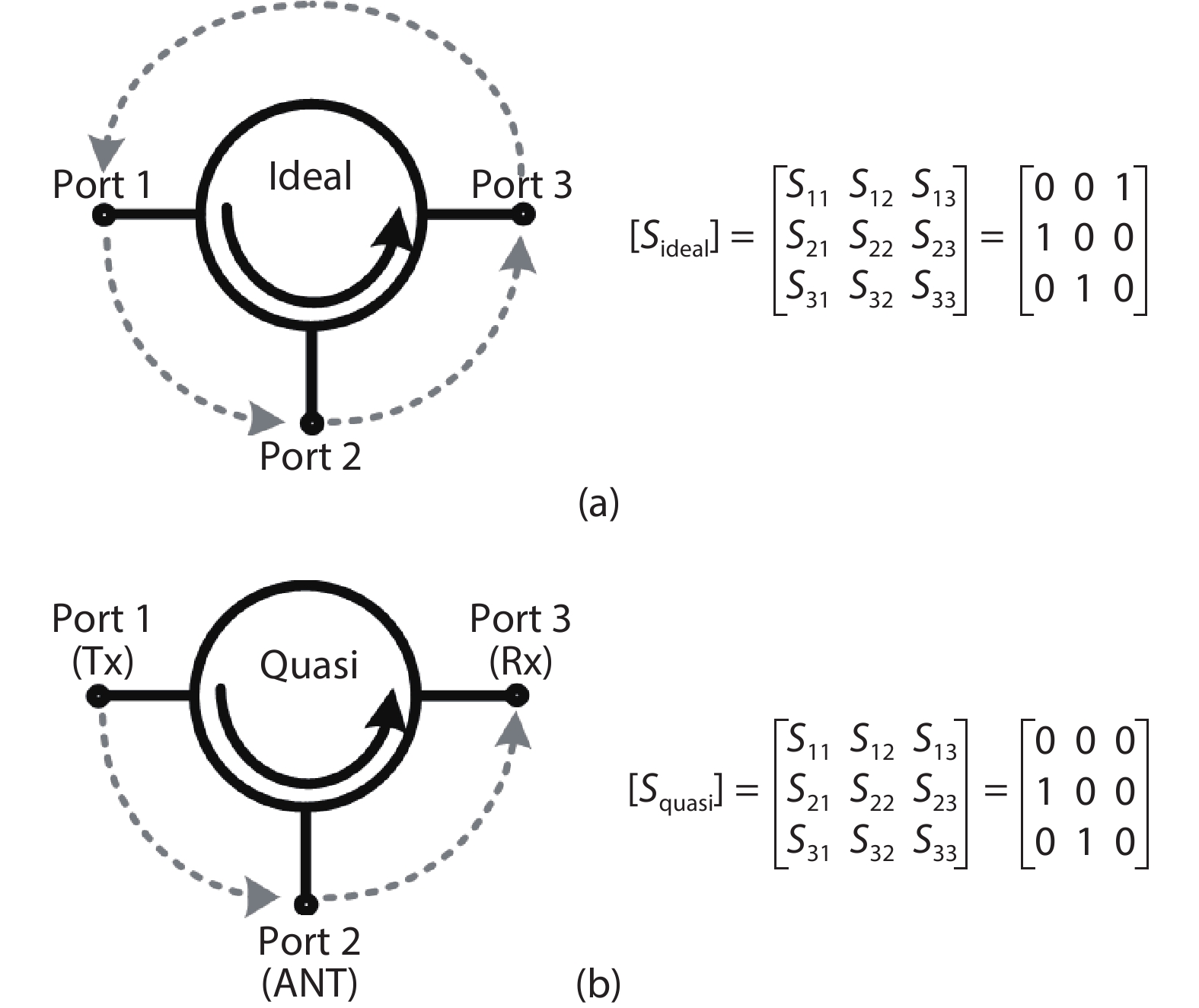
An ideal circulator with three ports is specified as |S21| = |S32| = |S13| = 1 and the other scattering parameters should be 0, as shown in Fig. 1(a). A quasi-circulator is a special type of circulator that two of its three ports (transmitter, receiver and antenna) are completely isolated in both clockwise and count-clockwise senses, as shown in Fig. 1(b), or |S13| = 0, which means that its receiver port is isolated from its transmitter port when it is used as a duplexer. As an alternative to their ferrite counterparts, active quasi-circulators possess the advantages of small size, light weight, low cost and compatibility with the monolithic wicrowave integrated circuit (MMIC) technology.
![]()
Figure 1.Diagrams showing the
In contrast to the multiple conventional devices, the tremendous growth of multi-band wireless communications stimulates the development of the compact and inexpensive single devices operating on multiple frequency bands, and each conventional device is assigned to a single frequency band. Circulators enable the system simultaneously transmitting and receiving the signals at different frequencies, which requires good port-to-port isolation, showing promise as an important component in wireless communication systems[
The active circulator is a key component in the future wireless systems and is responsible for multiplexing in the Tx/Rx circuits. When designing an active quasi-circulator, the key electrical parameters including frequency range, bandwidth, isolation, insertion loss, power handling, linearity and noise figure (NF) should be considered. At present, some methods and technical structures have been proposed and implemented to improve the performances of the active quasi-circulator.
2. Active quasi-circulators to improve isolation and broaden bandwidth
A common active quasi-circulator is based on phase cancellation structure[
![]()
Figure 2.(Color online) (a) Active quasi-circulator based on phase cancellation. (b) Core of conventional active quasi-circulator.
In order to improve the isolation performance over a wide bandwidth, especially the isolation of the Tx port (port 1) to the Rx port (port 3), i.e., S31, the tunable architectures and wideband architectures were proposed. These two main types of active quasi-circulators have their own advantages and disadvantages. The tunable active quasi-circulator can achieve high isolation performance but with limited bandwidth. In contrast, the wideband active quasi-circulator operates over a wide bandwidth, while the isolation S31 is usually not high enough.
2.1. Tunable architectures
The adjustable discrete components have achieved excellent narrow-band performance over a wide frequency range, which is common in quasi-circulators for multi-band wireless communication systems. By adding a tunable capacitor to a signal path of the circulator, as shown in Fig. 3(a), the capacitance value can be tuned according to the different frequencies to realize the adjustment of the phase of this path. By this way, the phase difference between the in-phase path and the out-of-phase path at different frequencies can be maintained near 180°, thereby ensuring the high isolation (S31). As shown in Fig. 3(b), high isolation can be obtained at multi-frequencies by tuning the capacitance. Fig. 3(c) shows the schematic of a tunable active quasi-circulator[
![]()
Figure 3.(Color online) (a) Active quasi-circulator with a tunable capacitor. (b) Isolation
The measured results show that the isolation (S31) exhibits nulls from 5.3 to 7.3 GHz ranging from 42 dB near the center frequency to 30 dB at the band edge, with a 20 dB cancelation bandwidth of 400 MHz. Tx gain (S21), RX insertion loss (S32), return losses (S11, S22, S33), and reverse isolation (S12) vary by less than 0.5 dB with respect to shunt capacitance.
Another tunable active quasi-circulator is shown in Fig. 4(a). The phase adjustment of the signal transmission path is realized by replacing the tunable capacitor with the T-network phase shifters. The detailed circuit structure of this tunable active quasi-circulator is shown in Fig. 4(b)[
![]()
Figure 4.(Color online) (a) Tunable active quasi-circulator with T-network phase shifters. (b) Schematic of the tunable active quasi-circulator by using DAs.
The measured tunable isolation between port 1 and port 3 shows wideband isolation with the minimum isolation of around 15 dB from 0.8 to 2.2 GHz, and the tunable isolation is more than 40 dB at ωo over the frequency range of 0.8–2.2 GHz. And the insertion losses and return losses are about 0 ± 1.5 dB and better than 10 dB, respectively.
Although the above two tunable active quasi-circulators obtain good isolation within a certain frequency range, the phase shifters based on tunable capacitor or T-network are narrowband devices. The corresponding bandwidth is still narrowed within near the specific adjustment point. The relatively narrow bandwidth does not satisfy the high data rate and large bandwidth requirements of 5G and future 6G wireless communications.
2.2. Wideband active quasi-circulators
To improve the isolation and bandwidth of the active quasi-circulator, the feedback technology[
2.2.1. Feedback technology
Feedback technology is commonly used in various circuit designs to increase the bandwidth and improve the circuit stability. In Ref. [21], the isolation from the transmitter to the receiver (S31) can be enhanced by adding a feedback path from port 3 to the cancellation signal path based on the common active circulator shown in Fig. 5(a). The circuit structure of the feedback active quasi-circulator is shown in Fig. 5(b), which is based on the conventional circuit structure shown in Fig. 2. M3 is added in the circuit to constitute a feed-back path.
![]()
Figure 5.(Color online) (a) Active quasi-circulator with feedback technology. (b) Core circuit of feedback active quasi-circulator.
According to Figs. 2 and 5, |S31c| of the conventional active quasi-circulator and |S31f| of the feedback active quasi-circulator are obtained, respectively, and can be expressed as[
where
The denominator part of |S31f| contains the square term of S in Ref. [21]. So when the frequency increases, the denominator increases fast, causing the value of |S31f| decrease more rapidly comparing with that of |S31c|, especially at the high frequency range[
The measured |S31| is higher than 27 dB over a frequency range from 0.8 to 6.8 GHz. The measured |S12| is higher than 15 dB, while |S23| and |S13| are all larger than 20 dB. The measured |S21| (insertion loss from Tx to antenna (ANT in Fig. 4)) is between −8 and −10 dB, while the measured |S32| (from antenna to Rx) is between −9 and −12 dB.
2.2.2. Dual technology
In order to further improve the isolation and bandwidth, the dual structure has been proposed, as shown in Fig. 6(a). Another cancellation signal (dual signal) is added in the dual structure, and the schematic of the dual interference-cancelling active quasi-circulator is shown in Fig. 6(c)[
![]()
Figure 6.(Color online) (a) Active quasi-circulator with dual technology. (a) Architecture of conventional active quasi-circulator. (b) Schematic of dual interference-cancelling active circulator.
The isolation from transmitter to receiver, represented by S31, is the most important performance of the active quasi-circulators. According to Figs. 6(b) and 6(c), |S31cc| of the conventional active quasi-circulator and |S31d| of the dual active quasi-circulator are obtained, respectively, and can be expressed as:
where Z1 = 1/gm1 + 1/C1S, Z1d = 1/gm1d + 1/C1dS, Z3 = RS + 1/CLS,Zad = RS + 1/CadS, and RS = 50 Ω. |S31d| is roughly improved by 2AB(E–F).
In addition, the two terms in Eq. (2), C and D, vary with frequency, resulting in cancellation within a relatively small frequency range, and hence a narrow isolation bandwidth. On the contrary, the two terms in Eq. (3), C – D and E – F, achieve a much better cancellation versus frequency, given that the circuits represented by the two terms are almost identical[
The measured isolation |S31| is better than 36 dB within bandwidth of 6 GHz. The measured insertion loss |S21| (from transmitter to antenna) and |S32| (from antenna to receiver) are below 10 and 9 dB from 1 to 7 GHz, respectively. Matching at Tx could be improved by adding additional impedance matching circuits.
2.2.3. Advanced dual technology
Due to the problem of large insertion loss and large noise figure of the dual active quasi-circulator[
![]()
Figure 7.(Color online) Architecture of advanced dual interference-cancelling active circulator.
The interference signal generated by the Tx signal through the out-of-phase path (M2) and the buffer (MB1) is suppressed by the cancellation signal generated from the Tx through the in-phase path (M1) and the buffer (MB2), which produces a residual signal. The dual cancellation signal is introduced in the advanced dual-path topology to further cancel the residual signal. The dual cancellation signal is generated by the Tx signal through the in-phase path (M1), the buffer (MB4), the out-of-phase path (M2E) and the buffer (MB3). The insertion loss is critical since the NF is partially dependent on it. The load resistor is degraded by both the finite output impedances of M1 and M2, and hence decreases the gain and deteriorates the NF[
The insertion losses of Ref. [24] and the advanced topology are given as S’32 and S32, respectively. Comparing S’32 with S32, Eq. (4) can be obtained
where Z'2 = 1/g’m2 + 1/C'aS, Z'L ≈ ro’1||ro’2||R', R' = 100 Ω, ro’1 ≈ ro’2 ≈ 500 Ω, Z2 = RS + 1/CaS, ZL = ro2||R2, R2 = 200 Ω, ro2 ≈ 500 Ω, RS = 50 Ω. Through the above analysis, S’32 < S32 can be obtained.
The isolation from Tx to Rx (S31) can be defined as the difference between the transmission losses from port 1 to port 2 (TX-ANT) and from port 1 to port 3 (TX-RX). The measured |S21| and S32| are below 8 and 2.5 dB from 1 to 8 GHz, respectively. The measured |S31| is better than 34 dB from 1 to 8 GHz. Compared with the dual technology, the advanced dual technology has improved |S21| and |S32| by 2 and 6.5 dB, respectively.
Although the above three technologies have effectively improved the isolation and the bandwidth of the active quasi-circulators, there are still problems of insufficient linearity, large insertion loss, and large noise figure. These problems will limit its application in 5G and future 6G communications.
3. Structures to improve power handling, linearity and noise figure (NF)
The most common approach adopted in the quasi-circulator designs to improve power handling, linearity and noise figure is based on the linear periodically-time-varying (LPTV) architecture[
![]()
Figure 8.(Color online) (a) LPTV active quasi-circulator. (b) Three-port circulator with a 3λ/4 transmission-line ring.
A 3λ/4 transmission line is wrapped around the N-path filter with 90° clock phase shift to create non-reciprocal wave propagation. In this ring, signals can only propagate in one direction. In the clockwise direction in Fig. 8(b)[
The measured in-band Tx-ANT and ANT-Rx IIP3 are 27.5 dBm and 8.7 dBm, respectively. The ANT-Rx NF is 4.3 dB, while the Tx-to-Rx isolation is better than 42 dB across 12 MHz bandwidth. The measured results show that the LPTV structure helps the active quasi-circulator to obtain relatively high linearity and relatively low NF.
Even though the active quasi-circulator based on the LPTV structure has good linearity, noise figure and high power processing capability, it cannot be used for broadband because of the narrowband characteristics of the LPTV structure. Therefore, it is not very suitable for the future high-speed and broadband wireless communications.
4. Comparison and future design trends of active quasi-circulators
Table 1 shows the comparison of the recently published active quasi-circulators, including the above mentioned six active quasi-circulators. For the wideband quasi-circulators[
With the development trend of the portable wireless communication systems, circulators should be miniaturized and highly integrated. Since ferrite passive circulators are large and difficult to be highly integrated, active quasi-circulators could be the mainstream of future development. And with the huge development of multi-band wireless communication, the circulator as an antenna interface must have the ability to work in broadband. Fig. 9 shows the bandwidth and isolation behaviors of the active quasi-circulator designs. Most active quasi-circulators are based on phase cancellation strategy. Since the phase difference and the amplitude of the signals vary with the frequency after the signals pass through the in-phase path and the out-of-phase path, most active quasi-circulators achieve high isolation within a limited bandwidth[
![]()
Figure 9.Bandwidth and isolation behaviors of state of art active quasi-circulators.
![]()
Figure 10.Linearity behaviors of state of art active quasi-circulators.
Therefore, to satisfy the performance of high isolation, broadband and high linearity at the same time presents a huge design challenge for active quasi-circulators in the future. Solving this problem will accelerate the full replacement of passive circulators by the active circulators, which will bring a great advancement in the high integrated wireless communication systems. Through analyzing the prior methods of how to improve the isolation, bandwidth, power processing, linearity and noise figure, discussing the compromise among the various performances and the performance distribution of the existing state of arts shown in Figs. 9 and 10, respectively, the following five aspects are feasible directions for the future research of active quasi-circulators, and all these aspects show great challenges.
(1) Expanding bandwidth. With the development of 5G communication and 6G communication in the future, the demands for broadband active quasi-circulators will increase rapidly. Most active quasi-circulators are based on phase cancellation. If the in-phase path and the out-of-phase path have the same frequency response, a large bandwidth can be obtained.
(2) Improving isolation. The circulator should have high degree of Tx-Rx isolation, which could greatly reduce the interference of the signal at transmitter to the signal at receiver, and will reduce the linearity requirement of the receiver. If the in-phase path and the out-of-phase path have the same amplitude response and the phase difference is exactly 180°, a very high degree of isolation can be guaranteed.
(3) Reducing insertion loss. Reducing the insertion loss of the active quasi-circulator will improve the transmission efficiency of the transmitter and save the power consumption, and will reduce the noise of the receiver. Reducing insertion loss can be achieved by adding buffers and power amplifiers in the output path, or by optimizing the circuit structure to reduce the loss on the signal transmission path.
(4) Improving linearity. Linearity is currently the key restriction of the passive circulators being replaced by the active quasi-circulators. The input reference P1dB of the active circulator needs to reach more than 30 dBm, which presents a very big challenge. The linearity can be improved by using high power-supply transistors or GaN devices, and the new structures like LPTV can also be used to improve the linearity.
(5) Reducing noise figure. The active quasi-circulator is the front end of the receiving link, and its noise contributes mostly to the noise figure of the entire link. Reducing the noise figure is another challenge in designing the active quasi-circulator. To reduce the noise figure, the design method similar to that of a low-noise amplifier can be adopted. On the one hand, the number of transistors on the signal transmission path should be reduced, and on the other hand, the gain on the signal transmission path need to be increased, and other noise cancellation technologies can also be applied.
5. Conclusion
As an antenna interface for multi-band wireless communications, the circulator must be capable to operate in multiple frequency bands, and at the same time it should have a large operating bandwidth. This survey reviews several existing structures of active quasi-circulators, and technical methods used to improve the bandwidth, isolation, linearity and noise performance. The advanced dual technology can effectively improve the isolation and bandwidth of the active quasi-circulator. The LPTV structure can be used to improve the linearity and noise performance. Better tradeoff among high isolation, broadband and good linearity needs to be made, which is always the direction of designing active quasi-circulators. Finally, the methods, which are useful to enhance the features of the active quasi-circulators, are provided to be the good references to the future works.
References
[1] A Fathy, E Denlinger, D Kalokitis et al. Miniature circulators for microwave superconducting systems. Proceedings of 1995 IEEE MTT-S International Microwave Symposium, 195(1995).
[2] E K N Yung, R S Chen, K Wu et al. Analysis and development of millimeter-wave waveguide-junction circulator with a ferrite sphere. IEEE Trans Microw Theory Tech, 46, 1721(1998).
[3] A M Borjak, L E Davis. More compact ferrite circulator junctions with predicted performance. IEEE Trans Microw Theory Tech, 40, 2352(1992).
[4] S W Y Mung, W S Chan. The challenge of active circulators: Design and optimization in future wireless communication. IEEE Microw Mag, 20, 55(2019).
[5] S Hara, T Tokumitsu, M Aikawa. Novel unilateral circuits for MMIC circulators. IEEE Trans Microw Theory Tech, 38, 1399(1990).
[6] S C Shin, J Y Huang, K Y Lin et al. A 1.5–9.6 GHz monolithic active quasi-circulator in 0.18
[7] H S Wu, C W Wang, C K C Tzuang. CMOS active quasi-circulator with dual transmission gains incorporating feedforward technique at K-band. IEEE Trans Microw Theory Tech, 58, 2084(2010).
[8] C H Chang, Y T Lo, J F Kiang. A 30 GHz active quasi-circulator with current-reuse technique in 0.18
[9] S W Y Mung, W S Chan. Novel active quasi-circulator with phase compensation technique. IEEE Microw Wirel Compon Lett, 18, 800(2008).
[10] A Gasmi, B Huyart, E Bergeault et al. Noise and power optimization of a MMIC quasi-circulator. IEEE Trans Microw Theory Tech, 45, 1572(1997).
[11] Y Zheng, C E Saavedra. Active quasi-circulator MMIC using OTAs. IEEE Microw Wirel Compon Lett, 19, 218(2009).
[12] C Kalialakis, M J Cryan, P S Hall et al. Analysis and design of integrated active circulator antennas. IEEE Trans Microw Theory Tech, 48, 1017(2000).
[13] M Palomba, A Bentini, D Palombini et al. A novel hybrid active quasi-circulator for L-band applications. 2012 19th International Conference on Microwaves, Radar & Wireless Communications, 41(2012).
[14] D J Huang, J L Kuo, H E Wang. A 24-GHz low power and high isolation active quasi-circulator. 2012 IEEE/MTT-S International Microwave Symposium Digest, 1(2012).
[15] S H Hung, Y C Lee, C C Su et al. High-isolation millimeter-wave subharmonic monolithic mixer with modified quasi-circulator. IEEE Trans Microw Theory Tech, 61, 1140(2013).
[16] S Wang, C H Lee, Y B Wu. Fully integrated 10-GHz active circulator and quasi-circulator using bridged-T networks in standard CMOS. IEEE Trans VLSI Syst, 24, 3184(2016).
[17] D Ghosh, G Kumar. A broadband active quasi circulator for UHF and L band applications. IEEE Microw Wirel Compon Lett, 26, 601(2016).
[18] S W Y Mung, W S Chan. Self-equalization technique for distributed quasi-circulator. Microw Opt Technol Lett, 51, 182(2009).
[19] S H Hung, K W Cheng, Y H Wang. An ultra wideband quasi-circulator with distributed amplifiers using 90 nm CMOS technology. IEEE Microw Wirel Compon Lett, 23, 656(2013).
[20] J Y Hsieh, T Wang, S S Lu. A 1.5-mW, 2.4 GHz quasi-circulator with high transmitter-to-receiver isolation in CMOS technology. IEEE Microw Wirel Compon Lett, 24, 872(2014).
[21] B J Tang, J T Xu, L Geng. Integrated active quasi-circulator with 27 dB isolation and 0.8–6.8GHz wideband by using feedback technique. 2018 IEEE MTT-S International Wireless Symposium (IWS), 1(2018).
[22] K Fang, J F Buckwalter. A tunable 5–7 GHz distributed active quasi-circulator with 18-dBm output power in CMOS SOI. IEEE Microw Wirel Compon Lett, 27, 998(2017).
[23] S W Y Mung, W S Chan. Wideband active quasi-circulator with tunable isolation enhancement. J Eng, 2014, 83(2014).
[24] B J Tang, X Y Gui, J T Xu et al. A dual interference-canceling active quasi-circulator achieving 36-dB isolation over 6-GHz bandwidth. IEEE Microw Wirel Compon Lett, 29, 409(2019).
[25] B J Tang, X Y Gui, J T Xu et al. A wideband active quasi-circulator with 34-dB isolation and insertion loss of 2.5 dB. IEEE Microw Wirel Compon Lett, 30, 693(2020).
[26]
[27] N Reiskarimian, J Zhou, H Krishnaswamy. A CMOS passive LPTV nonmagnetic circulator and its application in a full-duplex receiver. IEEE J Solid-State Circuits, 52, 1358(2017).
[28]
[29] S Jain, A Agrawal, M Johnson et al. A 0.55-to-0.9 GHz 2.7 dB NF full-duplex hybrid-coupler circulator with 56 MHz 40 dB TX SI suppression. 2018 IEEE International Solid-State Circuits Conference - (ISSCC), 400(2018).
[30]
[31]
[32] J Zhou, T H Chuang, T Dinc et al. Receiver with > 20MHz bandwidth self-interference cancellation suitable for FDD, co-existence and full-duplex applications. 2015 IEEE International Solid-State Circuits Conference (ISSCC), 1(2015).
[33] N Reiskarimian, J Zhou, T H Chuang et al. Analysis and design of two-port N-path bandpass filters with embedded phase shifting. IEEE Trans Circuits Syst II, 63, 728(2016).
[34] B van Liempd, B Hershberg, K Raczkowski et al. 2.2 A +70dBm IIP3 single-ended electrical-balance duplexer in 0.18
[35] D Yang, H Yuksel, A Molnar. A wideband highly integrated and widely tunable transceiver for in-band full-duplex communication. IEEE J Solid-State Circuits, 50, 1189(2015).
[36] A Nagulu, T J Chen, G Zussman et al. Non-magnetic 0.18
[37] S He, N Akel, C E Saavedra. Active quasi-circulator with high port-to-port isolation and small area. Electron Lett, 48, 848(2012).
[38]
[39]

Set citation alerts for the article
Please enter your email address
© Copyright 2018-2021 | Chinese Laser Press. All Rights Reserved 沪ICP备15018463号-20