• Laser & Optoelectronics Progress
  • Vol. 58, Issue 3, 3230011 (2021)
Teng Da1, Zhao Yongzhe1, Wang Yuncheng1, Li Yiqiang1, and Wang Kai2
Author Affiliations
  • 1College of Physics and Electronic Engineering, Zhengzhou Normal University, Zhengzhou , Henan 450044, China
  • 2Key Laboratory of Infrared Imaging Materials and Detectors, Shanghai Institute of Technical Physics, Chinese Academy of Sciences, Shanghai 200083, China
  • show less
    DOI: 10.3788/LOP202158.0323001 Cite this Article Set citation alerts
    Teng Da, Zhao Yongzhe, Wang Yuncheng, Li Yiqiang, Wang Kai. Graphene Plasmonic Waveguide Based on Silicon-on-Insulator Structure[J]. Laser & Optoelectronics Progress, 2021, 58(3): 3230011 Copy Citation Text show less
    Schematic of waveguide structure. (a) Three-dimensional structure; (b) two-dimensional cross section of waveguide structure
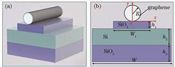
    Fig. 1. Schematic of waveguide structure. (a) Three-dimensional structure; (b) two-dimensional cross section of waveguide structure
    Normalized fundamental mode electric field distribution under different conditions. (a) Simulation results; (b) x direction; (c) y direction
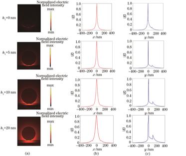
    Fig. 2. Normalized fundamental mode electric field distribution under different conditions. (a) Simulation results; (b) x direction; (c) y direction
    Relationship between mode characteristics and f. (a) neff; (b) LP; (c) Anor; (d) FOM
    Fig. 3. Relationship between mode characteristics and f. (a) neff; (b) LP; (c) Anor; (d) FOM
    Relationship between mode characteristics and R. (a) neff; (b) LP; (c) Anor; (d) FOM
    Fig. 4. Relationship between mode characteristics and R. (a) neff; (b) LP; (c) Anor; (d) FOM
    Relationship between mode characteristics and W1. (a) neff; (b) LP; (c) Anor; (d) FOM
    Fig. 5. Relationship between mode characteristics and W1. (a) neff; (b) LP; (c) Anor; (d) FOM
    Relationship between mode characteristics and μc. (a) neff; (b) LP; (c) Anor; (d) FOM
    Fig. 6. Relationship between mode characteristics and μc. (a) neff; (b) LP; (c) Anor; (d) FOM
    Crosstalk between adjacent structures. (a) Coupled system; (b) distribution of electric field component Ey in Ey,s and Ey,as; (c) distribution curves of the electric field component Ey in Ey,s and Ey,as along x direction; (d) normalized coupling lengths of different h1 values
    Fig. 7. Crosstalk between adjacent structures. (a) Coupled system; (b) distribution of electric field component Ey in Ey,s and Ey,as; (c) distribution curves of the electric field component Ey in Ey,s and Ey,as along x direction; (d) normalized coupling lengths of different h1 values
    Structuref/THzμc/eVAnor
    Ref.[25]501.01.35×10-3
    Ref.[34]301.0~1.00×10⁻⁴
    Ref.[35]30-500.6~1.00×10⁻⁵
    Ref.[37]200.67.00×10-5
    Proposed structure200.61.90×10-6
    Table 1. Model field area of different structures
    Teng Da, Zhao Yongzhe, Wang Yuncheng, Li Yiqiang, Wang Kai. Graphene Plasmonic Waveguide Based on Silicon-on-Insulator Structure[J]. Laser & Optoelectronics Progress, 2021, 58(3): 3230011
    Download Citation