
Siyu Zhou, Bo Peng. Non-volatile optical memory in vertical van der Waals heterostructures[J]. Journal of Semiconductors, 2020, 41(7): 072906
- Journal of Semiconductors
- Vol. 41, Issue 7, 072906 (2020)
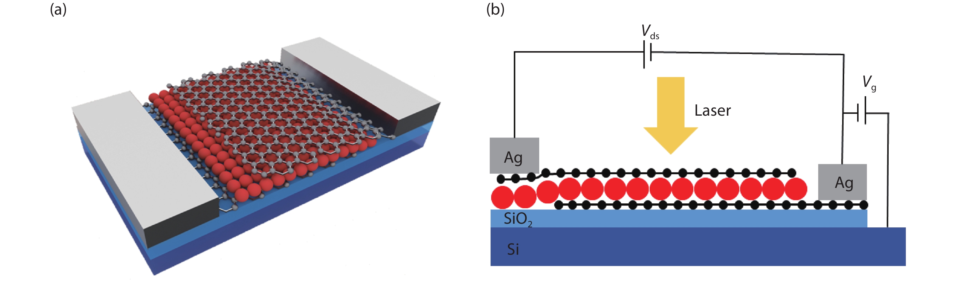
Fig. 1. (Color online) Device schematic. (a) Device with three-layer structure of graphene/CdSe QDs/graphene, silver as the electrodes on each graphene. (b) Circuit connection diagram of the devices.
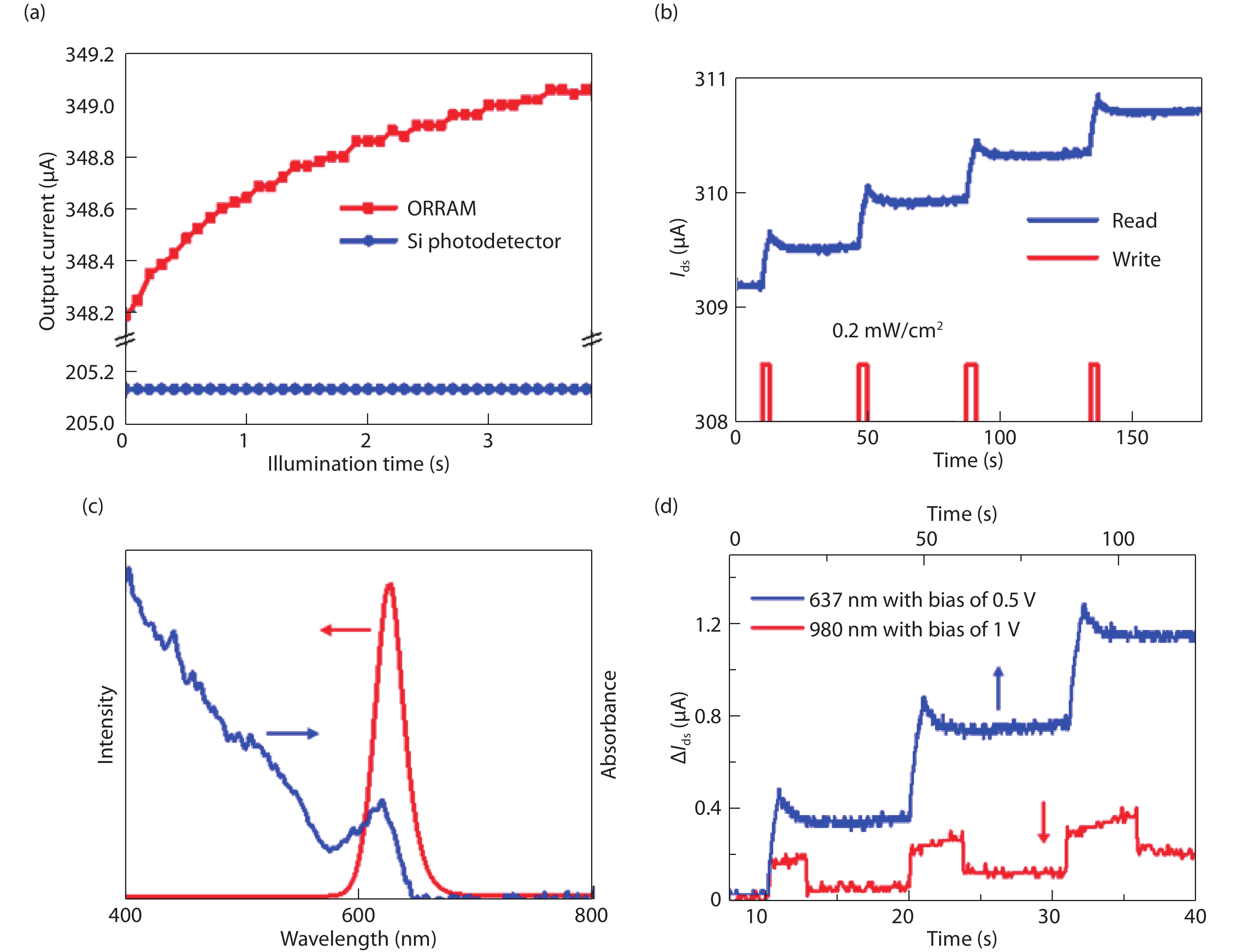
Fig. 2. (Color online) (a) Illumination time dependence of output current of a conventional commercial Si photodetector (blue) and our ORRAM synaptic device (red). (b) The non-volatile optical storage characteristic of the ORRAM device. A laser pulse of 637 nm with 0.2 mW/cm2 is used to write; a 0.5 V bias is applied to read. The pulse width is 3 s. (c) The absorption and photoluminescence spectra of CdSe QDs. (d) Under the light illumination at 980 and 637 nm, the relative increase of I ds of the device under three laser pulses respectively. Under 637 nm excitation, the photocurrent significantly increase, even the bias is halved.
Fig. 3. (Color online) (a) Band offset of Ag, graphene and CdSe QDs. (b) Energy band alignment of graphene and CdSe QDs in the heterojunctions. (c) The gate voltage dependence of I ds under bias of 1 V. (d) Schematic of electrons migration, accumulation and tunneling.
Fig. 4. (Color online) (a–c) The multi-level resistance states of the ORRAM device under different laser power and bias voltages. (d) Corresponding 2D mapping of ΔI ds as a function of bias voltages and laser power.
Fig. 5. (Color online) Storage state retention time of the device with bias of 1 V.

Set citation alerts for the article
Please enter your email address
© Copyright 2018-2021 | Chinese Laser Press. All Rights Reserved 沪ICP备15018463号-20