
Siyu Zhou, Bo Peng. Non-volatile optical memory in vertical van der Waals heterostructures[J]. Journal of Semiconductors, 2020, 41(7): 072906
- Journal of Semiconductors
- Vol. 41, Issue 7, 072906 (2020)
Abstract
1. Introduction
In the era of big data and artificial intelligence (AI), the demand for processing, memory and communication devices with higher speed, higher efficiency and lower power is becoming ever more urgent[
Non-volatile optical memory can directly sense, store, and process optical information in the same way as the neural network in the human visual system with light-tunable plasticity, which opens the door toward low-power artificial vision devices[
2. Experiment
2.1. Device design
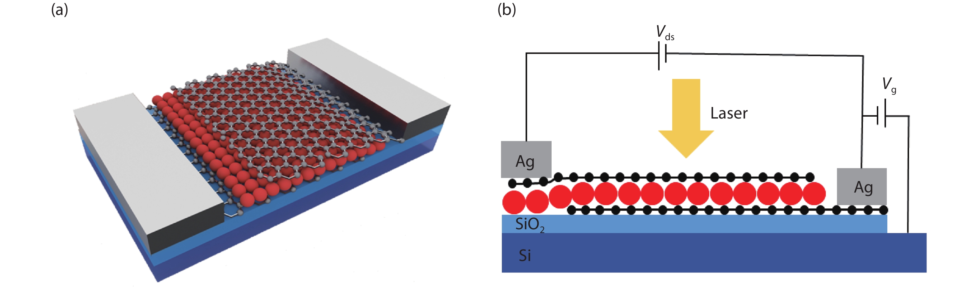
Fig. 1 shows a non-volatile optical memory with three-layer vertical heterostructure of graphene/QDs/graphene on Si/SiO2 substrate. In the two terminal symmetry ORRAM device, two monolayer graphene are used to sandwich a self-assembled monolayer CdSe QDs[
![]()
Figure 1.(Color online) Device schematic. (a) Device with three-layer structure of graphene/CdSe QDs/graphene, silver as the electrodes on each graphene. (b) Circuit connection diagram of the devices.
2.2. Device fabrication
CVD-grown graphene was spin-coated with PMMA and wet-transferred onto Si/SiO2 (285 nm) substrate, then acetone was used to remove the PMMA. The monolayer CdSe quantum dot (QD) was prepared by dropping CdSe QDs solution (10 μL) onto the surface of acetonitrile solvent[
3. Results and discussion
The resistance states of the ORRAM device can be tuned by optical stimulation. Displaying time-dependent and light-dosage-dependent behaviors opens the door to emulate the basic features of synaptic plasticity of the human brain. Fig. 2(a) shows the output current of a conventional commercial Si photodetector and our ORRAM synaptic device as a function of the illumination time. The photocurrent of Si photodetector remains constant. However, the output current of the ORRAM device is time-dependent, which increases with increasing illumination time. In many devices, a Schottky barrier may generate built-in electric field, which could drive the device[
![]()
Figure 2.(Color online) (a) Illumination time dependence of output current of a conventional commercial Si photodetector (blue) and our ORRAM synaptic device (red). (b) The non-volatile optical storage characteristic of the ORRAM device. A laser pulse of 637 nm with 0.2 mW/cm2 is used to write; a 0.5 V bias is applied to read. The pulse width is 3 s. (c) The absorption and photoluminescence spectra of CdSe QDs. (d) Under the light illumination at 980 and 637 nm, the relative increase of
Fig. 2(c) shows the absorption and photoluminescence spectra of CdSe QDs. The PL peak of CdSe QDs is at ~627 nm and the absorption cutoff wavelength is at ~650 nm, indicating that an illumination wavelength should be smaller than 650 nm to ensure the excitation of QDs layer. In Fig. 2(d), we show the relative increase of the current of the device under three laser pulses. When a laser at 980 nm is used to illuminate the device, the photocurrent dramatically decreases compared with the value upon excitation by 637 nm laser, even both the bias and laser power is increased by 1 time, from 0.5 V and 0.2 mW/cm2 to 1 V and 0.5 mW/cm2. Because laser of 980 nm below the absorption cutoff wavelength of QDs, resulting in that the QDs layer does not have any light absorption. The photocurrent under 980 nm excitation arise from the broadband photoresponse of graphene[
![]()
Figure 3.(Color online) (a) Band offset of Ag, graphene and CdSe QDs. (b) Energy band alignment of graphene and CdSe QDs in the heterojunctions. (c) The gate voltage dependence of
Previous studies have reported defect-induced non-volatile behaviors[
To further understand the mechanism, the effects of light intensity and bias on the synaptic behaviors are studied. Striking capacities of multi-level storage are observed (Figs. 4(a) and 4(b)). The increased laser power can induce increases of photogenerated carriers gathering at the interface states due to the Schottky barrier, while the increased bias voltage accelerates the carrier migration and tunneling. Thus, the output current and synaptic strengths of the ORRAM devices increase with increasing laser power and bias voltages, consistent with the mechanism in Fig. 3(d). Fig. 4(d) shows the corresponding 2D mapping of the ΔIds, ΔIds = IL – I0, where IL and I0 are the output current in the presence and absence of a pulsed laser illumination, respectively. The non-volatile resistance retention time of the ORRAM device is up to ~450 s after removing bias voltage (Fig. 5), which further confirm the stable long-term plasticity behaviors. The synaptic behaviors of the ORRAM devices can be tuned by light dosage and bias voltages, which allow us to design different strategies to emulate the features of synaptic plasticity to achieve the learning and memory functions of the human brain.
![]()
Figure 4.(Color online) (a–c) The multi-level resistance states of the ORRAM device under different laser power and bias voltages. (d) Corresponding 2D mapping of Δ
![]()
Figure 5.(Color online) Storage state retention time of the device with bias of 1 V.
4. Conclusion
In this work, we have proposed and demonstrated a non-volatile optical memory and synaptic behaviors in a three-layer vertical heterostructure of graphene/CdSe QDs/graphene. The ORRAM device exhibits multi-level memory capability and long storage time. The Schottky barrier between graphene and CdSe QDs introduces interface states to localize photo-induced carriers, leading to non-volatile optical memory. Furthermore, the low laser power and bias voltage reduce the energy consumption. This work shows great potential to apply 2D heterostructures in non-volatile optical memory and artificial neural networks.
Acknowledgements
We acknowledge financial support from National Science Foundation of China (51602040, 51872039), Science and Technology Program of Sichuan (M112018JY0025) and Scientific Research Foundation for New Teachers of UESTC (A03013023601007).
References
[1] M M Waldrop. The chips are down for Moore’s law. Nature, 530, 144(2016).
[2] G Indiveri, S C Liu. Memory and information processing in neuromorphic systems. Proc IEEE, 103, 1379(2015).
[3] S Cho, S H Tan, Z Li et al. SiGe epitaxial memory for neuromorphic computing with reproducible high performance based on engineered dislocations. Nat Mater, 17, 335(2018).
[4] J Lü, Y B Chen, Z Zuo et al. Charge storage characteristics of nonvolatile floating-gate memory based on gradual Ge1–
[5] H Y Zhou, H P Shi, B C Cheng. Surface traps-related nonvolatile resistive switching memory effect in a single SnO2:Sm nanowire. J Semicond, 41, 012101(2020).
[6] J Shen, J Cong, Y Chai et al. Nonvolatile memory based on nonlinear magnetoelectric effects. Phys Rev Appl, 6, 021001(2016).
[7] J Shen, J Cong, D Shang et al. A multilevel nonvolatile magnetoelectric memory. Sci Rep, 6, 34473(2016).
[8] S H Jo, T Chang, I Ebong et al. Nanoscale memristor device as synapse in neuromorphic systems. Nano Lett, 10, 1297(2010).
[9] C Li, M Hu, Y Li et al. Analogue signal and image processing with large memristor crossbars. Nat Electron, 1, 52(2017).
[10] D Zhu, Y Li, W Shen et al. Resistive random access memory and its applications in storage and nonvolatile logic. J Semicond, 38, 071002(2017).
[11] F Zhou, Z Zhou, J Chen et al. Optoelectronic resistive random access memory for neuromorphic vision sensors. Nat Nanotechnol, 14, 776(2019).
[12] L Britnell, R M Ribeiro, A Eckmann et al. Strong light-matter interactions in heterostructures of atomically thin films. Science, 340, 1311(2013).
[13] M D Tran, J H Kim, H Kim et al. Role of hole trap sites in MoS2 for inconsistency in optical and electrical phenomena. ACS Appl Mater Interfaces, 10, 10580(2018).
[14] H Yang, J Heo, S Park et al. Graphene barristor, a triode device with a gate-controlled Schottky barrier. Science, 336, 1140(2012).
[15] W Yu, Y Liu, H Zhou et al. Highly efficient gate-tunable photocurrent generation in vertical heterostructures of layered materials. Nat Nanotech, 8, 952(2013).
[16] X Wang, W Xie, J B Xu. Graphene based non-volatile memory devices. Adv Mater, 26, 5496(2014).
[17] F Zhou, J Chen, X Tao et al. 2D materials based optoelectronic memory: convergence of electronic memory and optical sensor. Research (Wash D C), 9490413(2019).
[18] Q Wang, Y Wen, K Cai et al. Nonvolatile infrared memory in MoS2/PbS van der Waals heterostructures. Sci Adv, 4, 7916(2018).
[19] S Chen, Z Lou, D Chen et al. An artificial flexible visual memory system based on an UV-motivated memristor. Adv Mater, 30, 1705400(2018).
[20] H Tan, G Liu, H Yang et al. Light-gated memristor with integrated logic and memory functions. ACS Nano, 11, 11298(2017).
[21] C G Kang, S K Lee, S Choe et al. Intrinsic photocurrent characteristics of graphene photodetectors passivated with Al2O3. Opt Express, 21, 23391(2013).
[22] B Peng, Z Li, E Mutlugun et al. Quantum dots on vertically aligned gold nanorod monolayer: plasmon enhanced fluorescence. Nanoscale, 6, 5592(2014).
[23] H Qiao, Z Huang, X Ren et al. Self-powered photodetectors based on 2D materials. Adv Opt Mater, 8, 1900765(2020).
[24] B Y Zhang, T Liu, B Meng et al. Broadband high photoresponse from pure monolayer graphene photodetector. Nat Commun, 4, 1811(2013).
[25] Y J Yu, Y Zhao, S Ryu et al. Tuning the graphene work function by electric field effect. Nano Lett, 9, 3430(2009).
[26] J Jasieniak, M Califano, S E Watkins. Size-dependent valence and conduction band-edge energies of semiconductor nanocrystals. ACS Nano, 5, 5888(2011).
[27] Y C Zhang, Y Y Shao, X B Lu et al. Defect states and charge trapping characteristics of HfO2 films for high performance nonvolatile memory applications. Appl Phys Lett, 105, 113(2014).
[28] K Cho, T Y Kim, W Park et al. Gate-bias stress-dependent photoconductive characteristics of multi-layer MoS2, field-effect transistors. Nanotechnology, 25, 155201(2014).
[29] A Bera, H Peng, J Lourembam et al. A versatile light-switchable nanorod memory: wurtzite ZnO on perovskite SrTiO3. Adv Funct Mater, 23, 4977(2013).
[30] J Lee, S Pak, Y W Lee et al. Monolayer optical memory cells based on artificial trap-mediated charge storage and release. Nat Commun, 8, 14734(2017).

Set citation alerts for the article
Please enter your email address
© Copyright 2018-2021 | Chinese Laser Press. All Rights Reserved 沪ICP备15018463号-20