• Journal of Semiconductors
  • Vol. 43, Issue 10, 103101 (2022)
Faraz Kaiser Malik* and Kristel Fobelets*
Author Affiliations
  • epartment of Electrical and Electronic Engineering, Imperial College London, SW7 2BT, nited Kingdom
  • show less
    DOI: 10.1088/1674-4926/43/10/103101 Cite this Article
    Faraz Kaiser Malik, Kristel Fobelets. A review of thermal rectification in solid-state devices[J]. Journal of Semiconductors, 2022, 43(10): 103101 Copy Citation Text show less
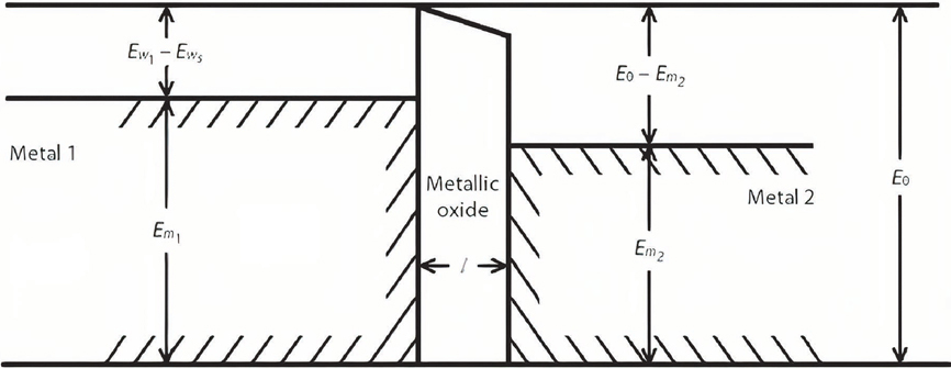
    Energy band diagram of an interface between dissimilar metals separated by a dielectric.Ews is the work function of the oxide layer, whileEwi andEmi represent the work function and Fermi level respectively of metali. Reprinted from Moon and Keeler[28], Copyright 1962, with permission from Elsevier.
    Fig. 1. Energy band diagram of an interface between dissimilar metals separated by a dielectric. Ews is the work function of the oxide layer, while Ewi and Emi represent the work function and Fermi level respectively of metali. Reprinted from Moon and Keeler[28], Copyright 1962, with permission from Elsevier.
    (Color online) Illustration of a thermal rectification system constituted of two materials with differing temperature dependence of thermal conductivity,κ under (a) forward and (b) reverse thermal bias. Reprinted with permission from Aroraet al.[42], Copyright 2017 by the American Physical Society.
    Fig. 2. (Color online) Illustration of a thermal rectification system constituted of two materials with differing temperature dependence of thermal conductivity, κ under (a) forward and (b) reverse thermal bias. Reprinted with permission from Aroraet al.[42], Copyright 2017 by the American Physical Society.
    (a) Illustration of the thickness-asymmetric graphene nanoribbon and (b) variation of the thermal conductivity of the specimen with temperature and grain orientation under forward and reverse thermal bias. Reprinted from Zhonget al.[56], with the permission of AIP Publishing.
    Fig. 3. (a) Illustration of the thickness-asymmetric graphene nanoribbon and (b) variation of the thermal conductivity of the specimen with temperature and grain orientation under forward and reverse thermal bias. Reprinted from Zhonget al.[56], with the permission of AIP Publishing.
    (Color online) Illustration of a thermally rectifying pillared graphene–monolayer graphene structure. Reprinted with permission from Yousefiet al.[57], © IOP Publishing.
    Fig. 4. (Color online) Illustration of a thermally rectifying pillared graphene–monolayer graphene structure. Reprinted with permission from Yousefiet al.[57], © IOP Publishing.
    (Color online) (a) Illustration of the asymmetric tilt grain boundary and (b) the resulting inequality in thermal conductivity of the specimen under opposing thermal bias. Reprinted from Caoet al.[58], Copyright 2012, with permission from Elsevier.
    Fig. 5. (Color online) (a) Illustration of the asymmetric tilt grain boundary and (b) the resulting inequality in thermal conductivity of the specimen under opposing thermal bias. Reprinted from Caoet al.[58], Copyright 2012, with permission from Elsevier.
    (Color online) (a) Illustration of the asymmetric graphene/h-BN heterostructures and (b) variation of the thermal rectification efficiency with the asymmetricity parameter. Note thatWLR=1.0 represents the geometrically symmetric case, and hBN-G represents the case where graphene is at the narrower end of the ribbon, and vice versa. Reprinted from Sandonaset al.[13], Copyright 2017, with permission from Elsevier.
    Fig. 6. (Color online) (a) Illustration of the asymmetric graphene/h-BN heterostructures and (b) variation of the thermal rectification efficiency with the asymmetricity parameter. Note that WLR=1.0 represents the geometrically symmetric case, and hBN-G represents the case where graphene is at the narrower end of the ribbon, and vice versa. Reprinted from Sandonaset al.[13], Copyright 2017, with permission from Elsevier.
    (Color online) (a) Illustration of the graphene/h-BN heterostructure, and the variation of the thermal rectification efficiency and (b) forward and reverse heat flux with the inter-layer coupling strengthχ. Adapted with permission from Chenet al.[51]. Copyright 2020 American Chemical Society.
    Fig. 7. (Color online) (a) Illustration of the graphene/h-BN heterostructure, and the variation of the thermal rectification efficiency and (b) forward and reverse heat flux with the inter-layer coupling strength χ. Adapted with permission from Chenet al.[51]. Copyright 2020 American Chemical Society.
    Illustration of the (a) monolayer graphene nanoribbon/silicon and (b) vertical carbon nanotube/silicon heterostructures. Reprinted from Vallabhaneniet al.[61], with the permission of AIP Publishing.
    Fig. 8. Illustration of the (a) monolayer graphene nanoribbon/silicon and (b) vertical carbon nanotube/silicon heterostructures. Reprinted from Vallabhaneniet al.[61], with the permission of AIP Publishing.
    (Color online) (a) Schematic illustration of the triangular and rectangular graphene nanoribbon geometries. (b) A comparison of the heat flux under forward and reverse thermal biasΔ withL=3.4 nm,Wbot=4.2 nm,Wtop=0.42 nm, andθ=60°, and (c) the resulting thermal rectification efficiency. ForΔ>0,TtopTbot. Reprinted from Yanget al.[69], with the permission of AIP Publishing.
    Fig. 9. (Color online) (a) Schematic illustration of the triangular and rectangular graphene nanoribbon geometries. (b) A comparison of the heat flux under forward and reverse thermal biasΔ with L=3.4 nm, Wbot=4.2 nm, Wtop=0.42 nm, and θ=60°, and (c) the resulting thermal rectification efficiency. ForΔ>0, Ttop<Tbot. Reprinted from Yanget al.[69], with the permission of AIP Publishing.
    (Color online) (a) Asymmetric geometrical MoS2 ribbon shapes. (b) Variation of temperature along the length of symmetric and trapezoidal nanoribbons with circles and squares representing forward and reverse thermal bias respectively. (c) Variation of the thermal rectification efficiency with geometrical asymmetricity for the three different ribbon shapes. (d) A comparison of the phonon participation ratios under opposing thermal biases for T-shaped ribbons withWLR=3.0. Reproduced from Sandonaset al.[72], with permission from the Royal Society of Chemistry.
    Fig. 10. (Color online) (a) Asymmetric geometrical MoS2 ribbon shapes. (b) Variation of temperature along the length of symmetric and trapezoidal nanoribbons with circles and squares representing forward and reverse thermal bias respectively. (c) Variation of the thermal rectification efficiency with geometrical asymmetricity for the three different ribbon shapes. (d) A comparison of the phonon participation ratios under opposing thermal biases for T-shaped ribbons with WLR=3.0. Reproduced from Sandonaset al.[72], with permission from the Royal Society of Chemistry.
    (Color online) (a) Thermal analysis of the three different geometrically asymmetric MoS2 nanoribbons in the forward bias direction and (b) comparison of the experimentally determined thermal rectification efficiency of the three structures calculated asη=(J+−J−)/J+. Recalculated value according to Eq. (1) presented inTable 1. Adapted with permission from Yanget al.[73], Copyright 2020 American Chemical Society.
    Fig. 11. (Color online) (a) Thermal analysis of the three different geometrically asymmetric MoS2 nanoribbons in the forward bias direction and (b) comparison of the experimentally determined thermal rectification efficiency of the three structures calculated as η=(J+J)/J+. Recalculated value according to Eq. (1) presented inTable 1. Adapted with permission from Yanget al.[73], Copyright 2020 American Chemical Society.
    (Color online) Illustration of the asymmetrically defective single-walled carbon nanotube, and the one-dimensional model used to simulate the system. Reprinted by permission from Springer Nature: Springer Journal of Mechanical Science and Technology, Hayashiet al.[76], Copyright 2011.
    Fig. 12. (Color online) Illustration of the asymmetrically defective single-walled carbon nanotube, and the one-dimensional model used to simulate the system. Reprinted by permission from Springer Nature: Springer Journal of Mechanical Science and Technology, Hayashiet al.[76], Copyright 2011.
    (Color online) A comparison of the thermal conductivity spectra for pristine graphene and 500 nm-long defective graphene. Reprinted with permission from Aroraet al.[42], Copyright 2017 by the American Physical Society.
    Fig. 13. (Color online) A comparison of the thermal conductivity spectra for pristine graphene and 500 nm-long defective graphene. Reprinted with permission from Aroraet al.[42], Copyright 2017 by the American Physical Society.
    (Color online) An illustration of the origin of thermal rectification in asymmetrically defective structures in terms of spatial asymmetry in the thermal conductivityλ. Reprinted from Wanget al.[19].
    Fig. 14. (Color online) An illustration of the origin of thermal rectification in asymmetrically defective structures in terms of spatial asymmetry in the thermal conductivity λ. Reprinted from Wanget al.[19].
    (Color online) Influence of thermal bias on the overlap in the phonon density of statesDp of graphene measured at a location before and after the defective region. Reprinted from Nobakhtet al.[78], Copyright 2018, with permission from Elsevier.
    Fig. 15. (Color online) Influence of thermal bias on the overlap in the phonon density of states Dp of graphene measured at a location before and after the defective region. Reprinted from Nobakhtet al.[78], Copyright 2018, with permission from Elsevier.
    (Color online) Influence of vacancy pattern modifications on the thermal rectification in micrometre-length silicon at room temperature. ‘Hierarchical’ indicates the presence of smaller pores between the larger ones, while ‘compressed’ refers to reduced interpore distances. Reprinted from Chakrabortyet al.[11], with the permission of AIP Publishing.
    Fig. 16. (Color online) Influence of vacancy pattern modifications on the thermal rectification in micrometre-length silicon at room temperature. ‘Hierarchical’ indicates the presence of smaller pores between the larger ones, while ‘compressed’ refers to reduced interpore distances. Reprinted from Chakrabortyet al.[11], with the permission of AIP Publishing.
    (Color online) Illustration of the experimentally determined thermal rectification in a porous silicon membrane. Adapted from Kasprzaket al.[82].
    Fig. 17. (Color online) Illustration of the experimentally determined thermal rectification in a porous silicon membrane. Adapted from Kasprzaket al.[82].
    Referenceη(%)Rectification StructureMechanism
    Giazotto & Bergeret[18]123Normal metal-superconductor nanojunctionElectronic thermal rectification
    Martinez-Perez & Giazotto[30]800Josephson tunnel junction
    Martinez-Perezet al.[31]13900Normal metal-insulator-superconductor junction
    Scheibneret al.[34]11GaAs/(Al,Ga)As QD
    Kuo & Chang[35]733Si/SiO2 QDs with vacuum layer between QD and metallic contact layers
    Zhang & Su[36]400Parallel-coupled double QD system
    Rogers[27]100Steel–aluminium interfaceGeometricallysymmetric interface between dissimilar materials
    Huet al.[40]45Silicon–amorphous polyethylene interface
    Kobayashiet al.[41]43LaCoO3–La0.7Sr0.3CoO3 interface
    Farzadianet al.[52]57Graphene–carbon nitride interface
    Liuet al.[54]36Monolayer graphene–silicene interface
    Caoet al.[58]74Armchair graphene–zigzag graphene interface
    Ordonez-Mirandaet al.[45]20PCM-based dissimilar material interface
    Pallecchiet al.[46]96
    Cottrillet al.[47]160
    Hirataet al.[48]170
    Kasaliet al.[49]150
    Zhonget al.[56]110Asymmetric thickness graphene nanoribbonOut-of-planegeometrical asymmetry across interface
    Yousefiet al.[57]5Pillared graphene–monolayer graphene interface
    Sandonaset al.[13]79Planar asymmetric graphene/h-BN nanoribbonsGeometrical asymmetry and dissimilar material interface
    Chenet al.[51]280Asymmetric thickness graphene/h-BN nanoribbons
    Vallabhaneniet al.[61]26Silicon–carbon nanotube/graphene nanoribbon interface
    Liet al.[62]90Double-walled graphene/h-BN nanotube
    Buiet al.[66]124Double-walled carbon nanotube
    Changet al.[67]7Asymmetrically mass-loaded nanotube
    Wanget al.[19]11Geometrically asymmetric graphene nanoribbonsGraded exterior geometry
    Yanget al.[69]350
    Huet al.[70]120
    Wanget al.[71]40
    Sandonaset al.[72]30Asymmetric molybdenum disulfide nanoribbons
    Yanget al.[73]233
    Hanet al.[74]168Weakly compressed 3D graphite nanocone
    Chakrabortyet al.[11]60Asymmetrically defective silicon structuresAsymmetricallydefectivesingle-materialstructures
    Kasprzaket al.[82]14
    Wanget al.[19]28Asymmetrically defective graphene structures
    Aroraet al.[42]233
    Nobakhtet al.[78]355
    Yousefiet al.[80]6
    Zhaoet al.[81]46
    Milleret al.[75]155Asymmetric pyramidal inclusions
    Hayashiet al.[76]60Asymmetrically defective single-walled carbon nanotubes
    Table 1. Comparison of the maximum thermal rectification efficiency reported according to Eq. (1) in previous literature using different rectification mechanisms.
    Faraz Kaiser Malik, Kristel Fobelets. A review of thermal rectification in solid-state devices[J]. Journal of Semiconductors, 2022, 43(10): 103101
    Download Citation