Abstract
Thermal rectification, or the asymmetric transport of heat along a structure, has recently been investigated as a potential solution to the thermal management issues that accompany the miniaturization of electronic devices. Applications of this concept in thermal logic circuits analogous to existing electronics-based processor logic have also been proposed. This review highlights some of the techniques that have been recently investigated for their potential to induce asymmetric thermal conductivity in solid-state structures that are composed of materials of interest to the electronics industry. These rectification approaches are compared in terms of their quantitative performance, as well as the range of practical applications that they would be best suited to. Techniques applicable to a range of length scales, from the continuum regime to quantum dots, are discussed, and where available, experimental findings that build upon numerical simulations or analytical predictions are also highlighted.Thermal rectification, or the asymmetric transport of heat along a structure, has recently been investigated as a potential solution to the thermal management issues that accompany the miniaturization of electronic devices. Applications of this concept in thermal logic circuits analogous to existing electronics-based processor logic have also been proposed. This review highlights some of the techniques that have been recently investigated for their potential to induce asymmetric thermal conductivity in solid-state structures that are composed of materials of interest to the electronics industry. These rectification approaches are compared in terms of their quantitative performance, as well as the range of practical applications that they would be best suited to. Techniques applicable to a range of length scales, from the continuum regime to quantum dots, are discussed, and where available, experimental findings that build upon numerical simulations or analytical predictions are also highlighted.Introduction
The rapid miniaturization of solid-state electronic devices over the past few decades has caused a drastic increase in on-chip transistor count, which has been accompanied by an exponential increase in power density[1,2]. Since thermal conductivity is reduced and static power losses increase with decreasing device dimensions, miniaturization accelerates the generation of localized thermal hotspots and can ultimately culminate in device breakdown[3–5]. Conventional cooling techniques are proving to be increasingly unsuitable for adequately addressing the high cooling demand of emerging electronic devices and guaranteeing system durability[6,7], with the development of efficient and compact thermal management solutions therefore being of significant interest.
Thermal rectification, a phenomenon where the heat flux through a structure changes as the temperature gradient across it is reversed[8], is particularly promising in this regard. It translates to preferential heat transport in one direction in a manner analogous to an electrical diode. Such behaviour has the potential to improve the thermoelectric properties of electronic devices, counter the formation of localized thermal hotspots caused by Joule heating, and improve device reliability. Thermal diodes may also be used as thermal insulators and safety elements within electronic circuits to prevent heat flow from hotspots along an undesirable direction in the circuitry. Furthermore, because most conceptualized thermal diodes are passive components, they can have the added benefit of eliminating the need for periodic recalibration associated with active thermal control systems used conventionally[9]. An improved understanding of thermal rectification and the development of thermal diodes also carries promise for the implementation of this concept in thermal logic circuits, memory, and energy storage systems.
Although thermal rectification will theoretically always exist in the presence of nonlinear interactions and broken inversion symmetry[10], the heat flux transmitted by a thermal diode in one direction must be appreciably different from that in the opposite direction for the device to be of practical significance. Spatially asymmetric heat flow properties are essential to achieve thermal rectification since modifications that uniformly enhance or degrade the mobility of electrons and phonons (energy carriers) in the system will not encourage unidirectional transport. The rectification strength is thus influenced by both the spatial and temperature dependence of thermal conductivity. For the purposes of comparison in this study, the thermal rectification efficiency
is defined as:
Here,
and
are the heat currents in the forward and reverse thermal bias directions respectively, and it is assumed that the heat flow is larger in the forward direction. Note that
represents the case where no thermal rectification occurs.
Analytical approaches are usually limited to the use of basic mathematical models with a significant number of simplifying assumptions, and to simple geometric configurations. Numerical methods, by contrast, are well suited for such investigations given their computational efficiency, flexibility, and inexpensiveness. Most studies on thermal rectification use either Monte Carlo or molecular dynamics simulations. The former uses empirical scattering probabilities to predict the behaviour of an ensemble of energy carriers[11], while the latter solve Newton’s equations of motion through separation distance dependent descriptions of interatomic force potentials[12]. These techniques allow for a wide variety of geometrical structures and materials to be simulated, because material parameters and force potential models can be modified with relative ease. Additionally, they eliminate the expense and complexities involved in experimental fabrication and testing, and the empirical nature of the employed models ensured high accuracy of results. However, experimental investigations on thermal rectification in nanoscale devices in literature are limited. They are confined to structures with larger characteristic feature sizes than in numerical studies, owing to limitations of fabrication and measurement capabilities requiring an isolated environment for accurate results[13].
This review summarizes and compares the techniques adopted to achieve thermal rectification in solid-state structures involving materials of interest to the electronics industry with a view to achieving simultaneous improvements in electrical and thermal characteristics. The influence of combining multiple rectification techniques is explored, and proposed applications of such thermal diodes are also discussed. For a wider range of techniques and applications of thermal rectification, including those involving convective and radiative heat transfer, readers are referred to reviews by Wehmeyeret al.[14] and Wonget al.[9]. Note that although mathematical definitions for the thermal rectification efficiency differ in published reports, this study adopts the convention of Eq. (1) to present a fair quantitative comparison, which is summarized in a tabular form in the conclusion section.
Thermal rectification mechanisms
Asymmetry in heat transport via any of the three mechanisms—conduction, convection, or radiation—can cause thermal rectification. In fluids confined between two horizontal parallel plates, for instance, the role of gravity and the resulting buoyancy effects result in preferential heat transport via convection against the direction of gravitational acceleration as hotter, less dense fluid tends to rise. Although most electronic cooling systems rely on convective heat transfer to exchange thermal energy with the environment, conduction is the dominant heat transfer mode within the circuitry at the individual component scale. Techniques to introduce asymmetric thermal conductivity are thus of particular significance in the context of solid-state devices.
Conductive thermal rectification was first reported by Starr[15], who noted through measurements that copper-cuprous oxide interfaces exhibit asymmetry in thermal conductivity as well as electrical conductivity. Interest in the applications of conductive thermal rectification and the construction of solid-state thermal diodes has since increased, with efforts undertaken to understand the origins of the phenomenon and develop structures to harness its potential. The following subsections describe the various approaches proposed for the achievement of thermal rectification through asymmetric heat conduction and discuss the underlying physical mechanisms behind the phenomenon.
Electronic rectification
A combination of electron and phonon transport contributes to the overall thermal conductivity within a material. Thermal rectification has been attributed to a range of causes that produce a mismatch in the directional mobilities of these energy carriers. These include geometrically asymmetric phonon confinement due to scattering events, spatial mismatch in phonon spectra, and electron energy filtering, to name a few[16–18]. Several of these factors may support each other and contribute concurrently to unequal heat flow under an equal but opposite thermal bias[19]. The vibrations of lattice atoms typically dominate over the contribution of electrons to thermal transport, particularly in semimetals and semiconductor materials that are most used in conventional electronics. Proposed techniques to achieve thermal rectification in solid state devices have thus mostly focused on inculcating an asymmetry in the phonon transport properties. However, interest has developed recently in controlling heat flow through selective filtering of electron transport, given the potential implications of such a design for simultaneous electronic and thermal rectification. Furthermore, this design can help improve the thermoelectric performance of the structure[20] and allow for the exploitation of phenomena such as Peltier cooling[21] to manage chip temperatures.
As aforementioned, the original observation of thermal rectification in solid-state devices by Starr[15] was based upon the asymmetry in thermal transport across a copper–copper oxide junction. Measurements indicated that both the thermal and electrical conductivity were higher for flow from the copper to the cuprous oxide than in the reverse direction, with a maximum reported rectification efficiency of 130%. Considering the electron theory of heat conduction, this observation was attributed to a mismatch in the energy transported across the interface in either direction by electrons, which are the primary carriers in metals. Subsequent studies on the thermal conductance across interfaces of conductors and non-conductors through electrons have highlighted two mechanisms: coupling between the electrons and phonons in the metal and nonmetal respectively[22,23], and coupling between electrons and phonons within the metal followed by coupling between the phonons on either side of the interface[24,25]. These studies have confirmed that since phonons are the primary energy carriers in the oxide region, the electrons must first transfer their energy to the phonons in the metal lattice, which subsequently transfer it across the interface to those in the oxide lattice while overcoming the interfacial resistance[22,24]. The thermal rectification effect in such metal–metal oxide junctions is thus interpreted in terms of the mismatch between the scattering rates when energy is transferred from electrons to phonons in the metal, and vice versa, near the interface.
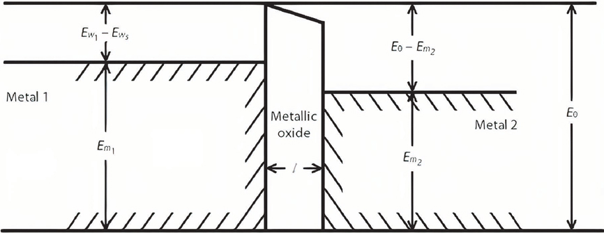
Thermal rectification due to asymmetric electron transport has also been reported across interfaces between metals with different work functions[26]. For instance, Rogers[27] experimentally demonstrated up to 100% thermal rectification across a steel–aluminium interface in a vacuum environment. Additionally, when separated by an insulating dielectric, as shown inFig. 1, such an interface between dissimilar metals results in the development of potential barriers of unequal magnitude at either side of the dielectric. Thus, depending on which side the electrons flow from, a different resistance to their motion is encountered, causing an unequal heat flux in opposite directions under a particular magnitude of applied external bias. The theoretical analysis performed by Moon and Keeler[28] confirmed preferential heat flow from the metal with the lower work function to that with the larger work function, because the potential barrier encountered by the electrons moving in this direction is smaller.
![Energy band diagram of an interface between dissimilar metals separated by a dielectric.Ews is the work function of the oxide layer, whileEwi andEmi represent the work function and Fermi level respectively of metali. Reprinted from Moon and Keeler[28], Copyright 1962, with permission from Elsevier.](/Images/icon/loading.gif)
Figure 1.Energy band diagram of an interface between dissimilar metals separated by a dielectric.
is the work function of the oxide layer, while
and
represent the work function and Fermi level respectively of metali. Reprinted from Moon and Keeler[28], Copyright 1962, with permission from Elsevier.
Such potential barriers are also encountered in Schottky contacts between metals and semiconductors. Controlling the electron flow through electronic transistors has thus been theorized as a potential mechanism to control heat transport. The total thermal conductivity of a lattice is constituted of the sum of the electronic and phononic contributions to heat transport. For elastic scattering in metals, the former is governed by the Wiedemann-Franz law as
, where
is the electrical conductivity,T is the absolute temperature, andL is the Lorenz number, given by the Sommerfield value[29]. However, as summarized in the review by Wehmeyeret al.[14], modulating the total thermal conductivity of a transistor by regulating the flow of electrons through gate control is not readily achievable. Ideally, for such an objective, it is desirable that the lattice contribution to heat transport is minimal, so that variations in the electronic contribution are carried over to the overall heat transport characteristics. Under conditions where the Wiedemann-Franz law is obeyed, an easily tuneable carrier concentration, as in moderately doped semiconductors, means that variations in the electronic thermal conductivity have a negligible impact on the overall conductivity of the device, because the lattice contribution is much higher. Meanwhile, in metals, where the carrier concentration is much higher and the electronic thermal conductivity far outweighs the contribution of phonons, the carrier concentration cannot easily be controlled by the gate and very large electric fields are required, making it difficult to achieve asymmetry in transport properties upon a reversal of thermal bias. As demonstrated by Crossnoet al.[29], conditions under which the Wiedemann-Franz law is violated and the electron thermal conductivity exceeds that defined by this relationship are thus potentially more conducive to electronic thermal rectification. At a temperature of 75 K, the electronic thermal conductivity of graphene was found to significantly exceed mathematical predictions and be particularly sensitive to the gate voltage through experimental measurements using the high-sensitivity Johnson noise thermometry technique. However, information about the phononic thermal conductivity was not collected, so conclusions regarding the variation (or lack thereof) of the total thermal conductivity could not be drawn.
Junctions between normal metals and superconductors have also been studied for their thermal rectification properties. Giazotto and Bergeret[18] theoretically predicted up to 123% electronic thermal rectification through nanojunctions between ballistic hybrid normal metal–superconductor contacts, with a hot terminal temperature equal to the superconducting critical temperature and ten times higher than the cold terminal temperature. For more realistic nanojunctions involving diffusive transport, this efficiency was determined to be as high as 84%. Meanwhile, Martinez-Perez and Giazotto[30] performed an analysis of the thermal rectification in Josephson tunnel junctions involving two different superconducting electrodes separated by an insulating barrier. Note that in both studies, the temperature sensitivity of the superconducting electronic density of states (DOS) contributed to the thermal rectification effect, and the phononic contribution to heat transport was neglected. In the latter study, where a maximum possible efficiency of 800% was determined, an inequality in the energy gaps of the two superconductors was identified to be essential for thermal rectification, with the quantum phase difference of the Cooper pair condensates also of importance. Moreover, through control over the phase bias as well as the hot terminal temperature relative to the superconductor critical temperature, the preferential heat flow direction of the proposed device could be switched.
Martinez-Perezet al.[31] subsequently fabricated a thermal diode involving a normal metal (Al0.98Mn0.02)–superconductor (Al) interface on a silicon wafer. Superconducting probes were tunnel-coupled to normal metal junctions separated by an insulating layer at either side of the central normal metal–insulator–superconductor segment, which could be operated as heaters or temperature sensors. The electrical characteristics of the device were shown to be independent of the applied voltage direction, but significant asymmetry in the electron temperature distribution under opposing thermal biases was measured at sub-Kelvin temperatures. The lattice phonons were assumed to be in thermal equilibrium and their contribution to heat flow was thus neglected, so the influence of asymmetry in electron transport properties on the overall thermal conductivity of the structure could not be definitively identified. For a substrate temperature of 50 mK and a thermal bias of 300 mK across the ends of the device, the heat current flowing from the normal metal towards the superconductor was found to be 140 times the heat current in the opposite direction upon a reversal of the terminal temperatures. Additionally, this rectification efficiency was found to decrease drastically as the substrate temperature was increased progressively from 50 to 300 mK, which confirmed that the constructed device would operate as a thermal rectifier only at cryogenic temperatures.
Recently, Breuniget al.[32] demonstrated analytically directional momentum filtering of electrons by an interface between a semiconductor with a low carrier density and a superconductor. Caused by a mismatch between the Fermi surfaces across the interface, it was found that electrons in the superconductor reaching the interface at incidence angles larger than a particular critical angle did not have corresponding modes in the semiconductor. These electrons were subsequently reflected without contributing to the transport of energy across the junctions. Interestingly, it was noted that the junction transmissivity could be limited to as few as a hundredth of all such incident electrons in practical junctions, with this filtering effect not encountered for flow in the reverse direction from the semiconductor to superconductor. Furthermore, unlike in normal metal–superconductor junctions, the transmissivity of the semiconductor–superconductor junction could be controlled through a gate voltage applied to the semiconductor. Although the thermal transport properties of this junction were not investigated, given the significant asymmetry in electron transport characteristics, electronic thermal rectification is highly likely to accompany the observed asymmetry in transport characteristics considering the results of previously discussed studies. Whether or not the electrons constitute a sufficiently significant portion of the total thermal conductivity as to cause such structures involving superconductors to behave as thermal rectifiers, and the conditions under which this occurs, requires further analysis because most investigations have neglected lattice thermal conductivity in their discussions.
Quantum dots (QDs), meanwhile, have attracted interest for thermoelectric applications due to their highly nonlinear transport properties in the Coulomb blockade regime[33]. Within the linear response regime of a 250 nm quantum dot fabricated using electron-beam lithography on a GaAs/(Al,Ga)As heterostructure, Scheibneret al.[34] noted thermal rectification characteristics under high magnetic fields applied in the plane of the two-dimensional electron gas. This rectification was concluded to arise due to asymmetric magnetic field dependence of the electronic energy states within the QD and its connecting leads. A rectification efficiency of up to 10.5% was recorded and found to be sensitive to the gate voltage, thereby allowing for modulation of the rectification properties without changes to the physical structure.
Kuo and Chang’s[35] subsequent theoretical study extended the analysis to the nonlinear response regime for silicon QDs embedded in amorphous silicon dioxide. Their device has a nanoscale vacuum layer between one electrode and the QD to suppress phonon thermal conductivity while allowing for electron tunnelling, thereby improving the thermoelectric figure of merit. If phonon conduction can be avoided in the support structure, then the proposed device could be used for thermal rectification up to room temperature, with 140 K a more realistic value in view of fabrication technology. While thermal rectification could not be predicted with certainty for a single QD structure, junctions involving two and three QDs were found to offer comparable rectification characteristics to each other, with the 3-QD junction allowing a higher maximum heat flux than the 2-QD structure. According to the definition of Eq. (1), a maximum rectification efficiency of 733% was reported for the 2-QD structure. This rectification was caused by strong electron Coulomb interactions between the QDs, in addition to the asymmetric QD–electrode coupling highlighted previously by Scheibneret al.[34]. To ensure the presence of these Coulomb interactions, an energy difference needs to exist between the QDs, with the rectification efficiency highly dependent upon the average occupancy of the lower-energy dot, but largely insensitive to that of the higher-energy QD. Similar results were reported recently by Zhang and Su[36] for a 2-QD junction involving parallel coupling of the quantum dots. By varying the coupling strength between the QDs and the electrodes within the theoretical model, they additionally reported that limiting the flow of electrons within the system through asymmetric coupling would confine the exchange of thermal energy to occur only through Coulomb interactions, and thereby enhance the thermal rectification efficiency. However, given the design of the structure, these results would only be applicable to sub-Kelvin operating temperatures where the phonon contribution to heat transport is negligible.
Interface effects
Due to the limited range of conditions under which the electronic contribution to thermal transport is large enough to influence the aggregate thermal conductivity, approaches to thermal rectification relying solely on the manipulation of electron flow remain less feasible. Techniques to inculcate rectification via asymmetric heat propagation through lattice vibrations are more readily applicable under typical operating conditions for electronic devices. One such alternate method to achieve inseparable temperature and spatial dependence of thermal conductivity is to create an interface between two structural regions with significantly differing temperature dependence of thermal conductivity[37], either due to differences in the constituent material, geometric design, or both.
Dissimilar materials
Early investigations into the thermal rectification effect caused by dissimilar lattices involved modelling the system as a chain of oscillators[38]. A sharp decrease in temperature was observed at the interface between the two dissimilar materials, which was attributed to the interface thermal resistance. This interface resistance was shown to be asymmetric under a reversal of the heat flux, and to strongly correlate to the overlap in the phonon spectra of the two materials. Furthermore, Liet al.[39] theorized that this asymmetry would vanish at very low temperatures, at which the lattices would lose their anharmonicity, and by extension, the temperature dependence of their phonon bands. A similar asymmetry in the interfacial thermal resistance was reported by Huet al.[40] for nanoscale silicon–amorphous polyethylene interfaces. Through molecular dynamics simulations, they demonstrated that softening of the polyethylene upon heating increases the number of long wavelength phonon modes available for heat transport. This improves the DOS overlap between the silicon and polyethylene regions, thereby reducing the interface resistance, and resulting in a thermal rectification efficiency of up to 45%.
As illustrated inFig. 2, when two dissimilar materials are brought into contact to create a heterojunction, the average thermal conductivity,
of a structure becomes a spatially asymmetric, nonlinear function of temperature. An advantage of this approach over the other phononic rectification techniques highlighted in the following sections is that it does not require nanostructures. Interfaces between dissimilar materials can potentially impose the necessary thermal conductivity variation even at the bulk scale due to the inherent mismatch in temperature dependence of
of the two materials. Kobayashiet al.[41], for instance, experimentally measured the temperature and heat flux in a sample made of two bulk-scale cobalt oxides, LaCoO3 and La0.7Sr0.3CoO3, joined together with a high thermal conductivity silver paste. The choice of materials was made based on their relatively low
, which helped maintain a high thermal gradient across the specimen, and their significantly differing temperature dependence. Up to 43% thermal rectification was recorded experimentally under a thermal bias of ΔT = 58.9 K, with the effect being credited to the different variation of
with temperature in the two materials rather than an asymmetry in the interfacial thermal resistance. In fact, it was noted that similarities in the lattice structure of the two oxides resulted in similar phonon dispersion properties and a negligibly small interfacial thermal resistance.
Figure 2.(Color online) Illustration of a thermal rectification system constituted of two materials with differing temperature dependence of thermal conductivity,
under (a) forward and (b) reverse thermal bias. Reprinted with permission from Aroraet al.[42], Copyright 2017 by the American Physical Society.
It is worth mentioning here that phase change materials (PCMs) have also been extensively investigated for their potential in thermal rectification[43,44]. Such proposals, which are essentially based upon the same concept as illustrated inFig. 2, exploit the drastic change in
that occurs upon a transition of phase. Within a small temperature window around the transition temperature,
thus changes akin to a step function rather than in the gradual manner shown inFig. 2[45]. Studies have confirmed that thermal rectification can be achieved through an interface either between a PCM and a phase-invariant material[45,46], or between two PCMs with differing conductivity responses to a change of state[47,48], with the latter offering greater design flexibility and performance efficiency. Given proper selection of the constituent materials, thermal rectification through PCMs is an attractive option because it allows for a high rectification efficiency to be achieved without large thermal biases at virtually any desired operating temperature, including room temperature. Kasaliet al.[49], for instance, demonstrated that a rectification efficiency of up to 30% could be achieved through a dual PCM diode using vanadium dioxide and polyethylene for a thermal bias of just 50 K, with the cooler end of the diode maintained at room temperature. Furthermore, PCM-based thermal rectification, which is based upon intrinsic material properties rather than any nanoscale phenomena, is achievable at the bulk scale. This allows for such rectifiers to be fabricated and characterized with relative ease in comparison to some of the other approaches to thermal rectification that are discussed later. However, implementation of this concept in modern electronic devices requires consideration of the change in electrical and thermal conductivity characteristics that may occur in PCMs upon miniaturization to the nanoscale. Additionally, the change of phase that is vital to the working of such rectifiers means that suitable containment of the liquified phase is essential to ensure device reliability, process reversibility, and safety of any sensitive components in the vicinity. Thermal expansion/contraction that occurs during phase change must also be accounted for in practical devices, because this can influence thermal contact area and device performance. The incorporation of such rectifiers to control heat flow in electronic circuits thus needs further investigation, but applications in thermal control systems, energy storage systems, and smart clothing seem viable.
Structures involving two-dimensional materials such as graphene and hexagonal boron nitride (h-BN) have also been the subject of extensive investigations recently as a potential simultaneous solution to the problems of heat flow control and electronic short-channel effects encountered in conventional solid-state devices. Layered materials offer the potential to engineer the thermal response and develop devices with tailored electrical and thermal properties through layer width modulation[50]. In conjunction with their attractive thermal conduction properties, this has garnered interest for low power applications. Studies have observed thermal rectification in two-dimensional materials of comparable magnitude to that in conventional semiconductors through similar transport modification techniques that introduce asymmetric thermal conductivity in electronic structures[13,51–53].
Interfacial thermal rectification in hybrid graphene/silicene monolayer ribbons was studied through molecular dynamics simulations by Liuet al.[54].
was observed to be higher when heat flowed from silicene into the graphene than in the opposite direction. Furthermore, the conductance was noted to vary with the system length up to 40 nm, beyond which negligible difference remained in the forward and reverse heat flux, indicating the contribution of nanoscale phenomena involving the phonon mean free path (MFP) to thermal rectification. A comparison of the phonon spectra of graphene and silicene revealed coupling between the phonons in silicene and the out-of-plane low frequency phonons in graphene. Furthermore, the phonon spectrum of graphene was shown to cover a much wider range of frequencies than that of silicene, meaning phonons travelling across the interface into graphene from silicene could be accepted. For heat conduction in the opposite direction, however, additional inelastic scattering events were required to decompose the high-frequency phonons originating in graphene into low-frequency phonons that could be accepted by silicene, leading to thermal rectification. Around 15% thermal rectification was observed at room temperature, which improved to 36% at 100 K. Improvements in the rectification efficiency were also noted by introducing strain into the silicene lattice, since silicene was shown to have a wider phonon MFP range (and thus a smaller mismatch with graphene) when relaxed.
Considering that the thermal conductivity of carbon nitride C3N is just under two-thirds that of graphene[55], Farzadianet al.[52] investigated the potential of thermal rectification in two-dimensional, geometrically symmetric graphene-C3N heterostructures. Through molecular dynamics simulations, it was confirmed that the interfacial thermal resistance changed with the direction of thermal bias due to unequal phonon scattering. The temperature sensitivity of the phonon DOS overlap translated to preferential heat flow from C3N to graphene, with up to 56.7% rectification in 40 nm-long structures subjected to a temperature difference of 100 K across their ends. The rectification efficiency was shown to improve with thermal bias, and to remain mostly unchanged with the sample length between 20 to 50 nm.
Geometrical discontinuity
For single-material structures, meanwhile, it has been demonstrated that thermal rectification may be achieved by exploiting the differing thermal conductivity characteristics that arise from a sudden change in the specimen thickness, and/or the grain boundary orientation. The former particularly holds true for interfaces between two regions of the same two-dimensional layered material of unequal thickness. Zhonget al.[56] demonstrated through molecular dynamics simulations that for the thickness-asymmetric graphene structure shown inFig. 3(a), heat flows preferentially from the monolayer to the multilayer region. In the reverse direction, the sudden constriction in cross-sectional area severely limits the transmissivity of phonons across the junction. Furthermore, the thermal rectification efficiency, reported to be as high as 110%, was shown to depend on both the average lattice temperature and the thickness ratio. At low thermal bias, a smaller thickness ratio was found to favour thermal rectification, with the opposite true at higher bias. Although thermal conductivity in either bias direction was reported to be higher in the armchair lattice orientation than its zigzag counterpart, as observable fromFig. 3(b), the thermal rectification efficiency was found to be largely independent of grain orientation in this case.
Figure 3.(a) Illustration of the thickness-asymmetric graphene nanoribbon and (b) variation of the thermal conductivity of the specimen with temperature and grain orientation under forward and reverse thermal bias. Reprinted from Zhonget al.[56], with the permission of AIP Publishing.
A similar approach exploiting the layered nature of graphene was adopted by Yousefiet al.[57]. Through molecular dynamics simulations, they demonstrated that an interface between monolayer and pillared graphene, as shown inFig. 4, could yield up to 5% thermal rectification in micrometre scale specimens, with preferential heat flow from the pillared region to the monolayer region. This observation was connected to the significantly lower thermal conductivity in pillared graphene compared to monolayer graphene, and the temperature-dependent scattering rate of long-wavelength phonons.
Figure 4.(Color online) Illustration of a thermally rectifying pillared graphene–monolayer graphene structure. Reprinted with permission from Yousefiet al.[57], © IOP Publishing.
Caoet al.[58], meanwhile, demonstrated that an asymmetric tilt grain boundary generated by connecting two separate ribbons of monolayer graphene, one in the armchair and another in the zigzag orientation, also exhibits thermal rectification characteristics. The interface between the two ribbons consisted of 5-pentagon and 7-heptagon topological defects, as illustrated inFig. 5(a). This device construction built upon the findings of earlier theoretical studies, which had demonstrated that significant differences exist between the phonon DOS of armchair and zigzag graphene[59,60]. Through molecular dynamics simulations, the temperature dependence of the DOS overlap was found to translate to a maximum thermal rectification efficiency of around 74% at room temperature, under a thermal bias of 120 K. As with most other reports on solid-state thermal rectifiers, this rectification efficiency was found to improve with a higher thermal bias, and to deteriorate upon an increase in the average lattice temperature.
Figure 5.(Color online) (a) Illustration of the asymmetric tilt grain boundary and (b) the resulting inequality in thermal conductivity of the specimen under opposing thermal bias. Reprinted from Caoet al.[58], Copyright 2012, with permission from Elsevier.
Combined material and geometric asymmetry
Studies on interfaces between geometrically asymmetric segments composed of dissimilar materials have additionally confirmed the occurrence of thermal rectification in such structures through combined contributions from the two factors. For instance, Sandonaset al.[13] combined the two separate approaches for thermal rectification across interfaces by performing simulations on geometrically asymmetric graphene/h-BN heterostructures. To understand the influence of the geometric discontinuity in addition to the material asymmetry on thermal rectification, the performance of a geometrically symmetric case was included in the comparison, and the material at the narrower end of the asymmetric structures was also swapped. Significantly,Fig. 6 indicates that thermal rectification of over 7.5% was recorded even in the geometrically symmetric ribbons, purely because of the differing temperature dependence of
of graphene and h-BN. In the geometrically asymmetric cases, preferential heat flow was noted in the direction of decreasing ribbon width, regardless of which material was at the narrower end, as also observed in Section 2.3. An overall improvement in rectification efficiency was recorded by combining the two techniques, which was particularly pronounced for the specimens with graphene at the narrower end of the ribbon. Unlike most rectification studies that are limited to simulations or measurements on suspended nanoribbons, the influence of graphite, silicon carbide, silicon and silicon dioxide substrates was also simulated. Substrates were found to increase the power spectrum overlap between graphene and h-BN through suppression of the out-of-plane phonon modes, and to reduce the rectification efficiency for ribbons with small geometrical asymmetricity. However, for highly asymmetric structures, the rectification efficiency improved after deposition on a substrate, with a maximum efficiency of 24% being recorded. Additionally, lower substrate temperatures were demonstrated to be favourable for thermal rectification, with up to 79% efficiency being reported for geometrically symmetric h-BN/graphene on a silicon substrate at 100 K. Graphite, meanwhile, proved to be the worst substrate material for thermal rectification. In light of these results, the authors concluded that control of the substrate temperature was more critical to thermal rectification in such heterojunctions than geometric asymmetricity, which can be hard to achieve in fabricated specimens.
Figure 6.(Color online) (a) Illustration of the asymmetric graphene/h-BN heterostructures and (b) variation of the thermal rectification efficiency with the asymmetricity parameter. Note that
represents the geometrically symmetric case, and hBN-G represents the case where graphene is at the narrower end of the ribbon, and vice versa. Reprinted from Sandonaset al.[13], Copyright 2017, with permission from Elsevier.
Chenet al.[51] extended the work by simulating the performance of the graphene/h-BN heterostructure shown inFig. 7. A portion of monolayer graphene was sandwiched between h-BN layers through van der Waals (vdW) bonds. As with the structure investigated by Zhonget al.[56], preferential heat flow was noted from the monolayer to the multilayer region. The influence of the vdW bonds was found to result in strong directional dependence of the out-of-plane phonon DOS overlap, and to also modify the coupling between in-plane and out-of-plane phonons. Upon an increase in the interlayer coupling strength, the suppression of low frequency phonons in the encased graphene was enhanced, while the phonon spectrum of the monolayer graphene was predictably unchanged. This subsequently meant that heat transfer from h-BN to graphene under reverse thermal bias was more adversely impacted than in the opposite direction. Accordingly, the larger inequality in the spectral overlap under opposing thermal biases made for an improved thermal rectification efficiency. An increase in the number of encasing h-BN layers, however, contributed to a deterioration in rectification efficiency, as did an increase in the point defect density. Critically, it was shown that rectification is reduced with an increase in the sample length, and becomes negligible for lengths over 53.3 nm, confirming that the physical mechanism behind the existence of the phenomenon in such asymmetric thickness junctions is not applicable at the bulk scale.
Figure 7.(Color online) (a) Illustration of the graphene/h-BN heterostructure, and the variation of the thermal rectification efficiency and (b) forward and reverse heat flux with the inter-layer coupling strength
. Adapted with permission from Chenet al.[51]. Copyright 2020 American Chemical Society.
Simulations on the interfaces between vertical carbon nanotubes or graphene nanoribbons and silicon performed by Vallabhaneniet al.[61], as shown inFig. 8, also confirmed thermal rectification in these structures that involved both material and geometric asymmetry. The filling fraction, or the ratio of the actual nanotube-silicon contact area to the entire substrate area, was found to be important to the interfacial thermal resistance, since a larger filling fraction corresponds to a larger cross-sectional area for heat flow across the interface. The thermal conductance was observed to be higher for heat flow from the nanotubes to the substrate, because the reduction in flow area in the reverse direction adversely impacted the overall transport property. Up to 26% thermal rectification was noted, with larger filling fractions reducing the asymmetry in thermal conductivity by addressing the mismatch in cross-sectional area across the interface.
Figure 8.Illustration of the (a) monolayer graphene nanoribbon/silicon and (b) vertical carbon nanotube/silicon heterostructures. Reprinted from Vallabhaneniet al.[61], with the permission of AIP Publishing.
Through molecular dynamics simulations, Liet al.[62] investigated the thermal transport properties of a stacked graphene/h-BN bilayer structure, as well as a coaxial carbon/boron nitride nanotube. Such heterostructures based on vdW interactions have previously been proposed for use in tunnelling rectifiers[63], thermoelectric devices[64] and graphene-based field-effect transistors[65]. Interestingly, for the bilayer heterojunction, no significant thermal rectification was recorded across the vdW-based h-BN/graphene interface, with the interfacial thermal resistance found to be insensitive to the direction of thermal bias. This was due to a significant overlap in the DOS of h-BN and graphene made possible by absolute lattice matching within the layered heterojunction and the similar phonon spectra of the two constituent materials. Despite a reduction in the thermal resistance with an increasing lattice temperature, this variation was equal under both thermal bias directions, and consequently, no significant asymmetricity in the transport properties was observed. This contrasts with the findings of Sandonaset al.[13] for covalently bonded, in-plane h-BN/graphene junctions, where the temperature sensitivity of the DOS overlap caused thermal rectification even in geometrically symmetric structures. However, for the concentric double-walled nanotubes involving a circular vdW-based interface, up to 90% thermal rectification was reported by Liet al.[62]. Preferential heat flow radially inwards was reported, regardless of whether the carbon or boron nitride nanotube was of smaller diameter. Also noted in double walled nanotubes by Buiet al.[66], this behaviour was explained by the improved mechanical coupling that results from an expansion of the inner nanotube upon heating and the simultaneous contraction of the outer nanotube as it loses heat, as opposed to the weakened coupling caused by heat flow in the opposite direction. Although the phonon spectra of vdW-bonded graphene and h-BN in the two-dimensional stacked heterostructure were found to be similar and insensitive to the bias direction, in the concentric nanotube arrangement, the outer tube (irrespective of material) was found to have a larger concentration of high-frequency phonons than the inner tube. The phonon population in the outer nanotube can thus carry more energy across the interface than in the reverse direction, thereby causing thermal rectification.
The thermal conductivity of nanotubes subjected to inhomogeneous external mass-loading with heavy molecules has also been shown to vary with the axial location, with higher heat flow recorded in the direction of decreasing mass density[67]. In a modified version of this approach, Desmarchelieret al.[68] performed molecular dynamics and wave-packet propagation simulations on 50–100 nm-long core/shell nanowires with a core of crystalline silicon 5 nm in diameter, and an amorphous silicon shell of varying shape. Different opening angles for the shell geometry were considered, with a larger angle corresponding to greater variation in the shell thickness along the axial length of the nanowire. Simulations predicted that the rate of heat transfer would be higher in the direction of increasing shell thickness than in the reverse direction due to the combined influence of the asymmetric material interface and the variation of the nanowire mass along its length. The transport characteristics of low-frequency phonons were particularly found to be influenced by the shell shape and the interface between the crystalline and amorphous silicon running parallel to the direction of heat conduction. While this observation regarding the preferred direction of heat flow conflicts with previous reports on externally loaded nanowires and the geometrically asymmetric nanoribbons discussed earlier, the differences between the length scales and materials involved in the structures investigated in literature mean that further investigations are necessary to confirm the origin of this discrepancy.
Graded exterior geometries
As aforementioned, the achievement of thermal rectification in solid structures requires
to vary as a function of both temperature and spatial location. While this is more straightforward to achieve through an interface between dissimilar materials, as in the original observation of Starr[15], studies have since shown that rectification can also be achieved in planar structures composed of a single material. The introduction of geometrical irregularities has been shown to help invoke spatial dependence in the material properties, and a graded exterior geometry has been proposed as one of the simplest means of achieving thermal rectification.
Yanget al.[69] employed classical non-equilibrium molecular dynamics simulations to investigate the characteristics of heat flow through geometrically asymmetric graphene nanoribbons. Two distinct ribbon shapes were considered as shown inFig. 9(a): a triangular ribbon in which the width decreases continuously as a function of length, and a step-type ribbon consisting of two rectangular segments of differing thicknesses. As shown inFig. 9(b), heat was observed to flow preferentially from the wider to the narrower region for both geometric configurations. This rectifying behaviour was predicted to be due to the variation in the transversal ribbon size causing a difference in the localization of high-frequency phonon modes under forward and reverse thermal bias. Furthermore, as observable fromFig. 9(c), it was found that the triangular ribbon exhibits greater thermal rectification under the same thermal bias, which was credited to the continuous mismatch in phonon spectra that occurs throughout the length of the triangular ribbon as opposed to only at the junction for the rectangular case.
Figure 9.(Color online) (a) Schematic illustration of the triangular and rectangular graphene nanoribbon geometries. (b) A comparison of the heat flux under forward and reverse thermal biasΔ with
nm,
nm,
nm, and
°, and (c) the resulting thermal rectification efficiency. ForΔ,
. Reprinted from Yanget al.[69], with the permission of AIP Publishing.
A similar study was performed by Huet al.[70], who compared the thermal transport characteristics of geometrically symmetric and asymmetric graphene nanoribbons with lengths of up to 10 nm. No thermal rectification was observed in symmetric rectangular ribbons but results similar to those of Yanget al.[69] were reported for asymmetric ribbons constructed as right-angled triangles. Upon studying the influence of edge chirality and geometric modifications, it was found that nanoribbons with armchair bottom edges and a 30° vertex angle offer the best thermal rectification characteristics. This was despite ribbons with zigzag edges offering higher thermal conductivity, and both irregular edge scattering and large vertex angles were reported to decrease the thermal rectification. Additionally, the random introduction of circular vacancies and edge roughness in the pristine ribbons adversely impacted both the thermal conductivity and rectification by causing a uniform increase in boundary scattering events and thereby reducing the role of the asymmetric external geometry in limiting lattice thermal conductivity. The following section discusses the impact of such defects on thermal rectification in further detail.
Wanget al.[71] confirmed through molecular dynamics simulations that thermal rectification in such geometrically asymmetric graphene nanoribbons is caused by phonon confinement in the lateral direction. This confinement effect in turn encourages three different but interconnected mechanisms for thermal rectification: unequal phonon spectra overlap under opposing bias conditions, phonon edge localization, and inseparable dependence of thermal conductivity on both temperature and spatial location. Consequently, thermal rectification decreases as the width of the nanoribbons is increased because the significance of lateral phonon confinement over scattering events encountered along the transport direction diminishes, and the lack of rectification in bulk-size geometrically asymmetric homogenous single-material structures was verified in this study.
This approach to thermal rectification was subsequently extended by Sandonaset al.[72] to the asymmetric single-layer molybdenum disulfide (MoS2) nanoribbons shown inFig. 10(a). They reported that, like in graphene, the temperature of the wider end of the ribbon determines its average temperature, as illustrated inFig. 10(b) by the profiles of temperature in trapezoidal ribbons under opposing thermal biases. Furthermore, the rectification efficiency was found to improve with increasing geometric asymmetry (represented by the parameter
) due to an increasing difference in the number of lattice atoms interacting with the heat baths placed at either end of the nanoribbons to maintain the constant heat flux during the simulations. Interestingly, in a departure from the previous observations on graphene by Huet al.[70], it was noted that T-shaped MoS2 ribbons exhibit significantly higher rectification efficiencies compared to their triangular and trapezoidal counterparts of the same length, as observable inFig. 10(c). An analysis of the vibrational density of states revealed that structural asymmetries and finite cross-sectional area of the ribbons together cause strong localization of the high frequency phonons and limit their participation in thermal transport.Fig. 10(d) indicates increased localization among the high frequency modes under reverse bias conditions, with the low and medium frequency modes exhibiting similar participation ratios and thus not contributing to thermal rectification. Upon further investigation, this trend was attributed to the influence of heat flow direction upon the sulfur atoms within the bulk of the lattice, with the contribution of atoms along the edges and that of molybdenum atoms found to be largely unaffected by a reversal in heat flow.
Figure 10.(Color online) (a) Asymmetric geometrical MoS2 ribbon shapes. (b) Variation of temperature along the length of symmetric and trapezoidal nanoribbons with circles and squares representing forward and reverse thermal bias respectively. (c) Variation of the thermal rectification efficiency with geometrical asymmetricity for the three different ribbon shapes. (d) A comparison of the phonon participation ratios under opposing thermal biases for T-shaped ribbons with
. Reproduced from Sandonaset al.[72], with permission from the Royal Society of Chemistry.
The thermal rectification predicted in asymmetric graphene nanostructures by the simulation-based studies discussed earlier was verified experimentally by Wanget al.[19]. Tapered CVD grown graphene nanoribbons were completely suspended between two metallic sensors. Either sensor could then be used as a heater or thermometer. The H-type sensor method was used, as it offers high measurement accuracy and allows the direction of heat flux to be reversed. Note that due to the limitations on minimum physical ribbon size imposed by fabrication and measurement capabilities, and the computational cost associated with large numerical models, the length scales of the experimentally investigated ribbons in this study were two orders of magnitude larger than those considered through molecular dynamics simulations. Nonetheless, the experiments confirmed up to 11% higher preferential heat flow from the wider to the narrower end of trapezoidal nanoribbons compared to the opposite direction, with simulations predicting a logarithmic increase in the rectification efficiency with decreasing ribbon width. Further investigations revealed that the increased edge scattering near the narrower end causes the increased phonon localization noted previously. Compounded with the fact that phonon population density increases with local temperature, this means that under reverse thermal bias, where the narrower end is hotter, the edge scattering reduces the MFP for a larger number of phonons than under the forward bias condition, thereby culminating in rectification.
Similarly, thermal rectification in geometrically graded, suspended monolayer MoS2 nanoribbons was experimentally confirmed by Yanget al.[73]. The heat transfer rate and resulting temperature variation over the length of the three different asymmetric ribbon geometries shown inFig. 11(a) was measured after their fabrication, and the corresponding thermal conductivity calculated. By repeating this procedure for the opposite heating direction, the thermal rectification efficiency of the structures was determined and found to be largely insensitive to the applied external heat flux, as illustrated byFig. 11(b). As predicted by previous simulation-based studies, a higher thermal conductivity was recorded in the direction of narrowing width for all three manufactured specimens, despite their considerably different sweep profiles. Although the authors credited this phenomenon to merely the difference in contact area with the heat bath at either end of the ribbon, considering that the comparisons between the forward and reverse bias directions were performed at equal heating powers, this would mean that the heat flux was, in fact, larger at the narrow end of the ribbon. As aforementioned, Sandonaset al.[72] demonstrated that thermal rectification in geometrically asymmetric MoS2 nanoribbons is caused by a modification of the phonon spectra, which has also been proven for similar nanoscale structures made of other materials.
Figure 11.(Color online) (a) Thermal analysis of the three different geometrically asymmetric MoS2 nanoribbons in the forward bias direction and (b) comparison of the experimentally determined thermal rectification efficiency of the three structures calculated as
. Recalculated value according to Eq. (1) presented inTable 1. Adapted with permission from Yanget al.[73], Copyright 2020 American Chemical Society.
Furthermore, molecular dynamics simulations have demonstrated that thermal rectification can also be achieved in three-dimensional nanocones. Hanet al.[74] investigated the thermal performance of graphite nanocones in two different crystallographic orientations, which had a triangular cross-section like that of the two-dimensional triangular nanoribbons investigated by previous researchers. A mismatch in the phonon DOS was recorded between adjacent graphene layers within the nanocone, and the involvement of weaker vdW interactions between the layers resulted in a mismatch between the in-plane and out-of-plane spectra as well. The phonon DOS overlap between the individual graphene layers constituting the nanocone, and by extension, the overall thermal conductivity of the structure was thus sensitive to the crystallographic orientation, layer stacking pattern, and lattice temperature. A rectification efficiency of up to 101% was recorded in the range of conditions investigated, which could be improved to 168% upon the application of a weak compressive stress.
Given the origins of thermal rectification in such geometrically asymmetric nanostructures composed of a single material, the finite width of the nanoribbons is an essential factor determining the rectification efficiency. As the width increases, the phonon participation ratio ceases to be a function of the lateral dimension and depends only on temperature[71]. This eliminates the spatial dependence of DOS overlap and thermal conductivity that is essential to causing unequal heat flow in opposing directions. Furthermore, the rectification efficiency was generally noted to improve with increasing geometric asymmetry[69,72], increasing thermal bias[69,71], reduced average lattice temperature[70,74], and shorter system lengths[69,72,74].
Asymmetric structural defects
At length scales smaller than the phonon MFP, the energy carrier transport properties can be modified artificially through inclusions or defects within device structures causing spatially asymmetric and temperature dependent phonon scattering. Milleret al.[75] adopted a combination of a Landauer-Buttiker method and a Monte Carlo technique to model the thermal transport in nanostructures. It was demonstrated that asymmetry in ballistic phonon scattering caused by pyramidal inclusions within the device results in thermal rectification. Due to the geometry of these inclusions, phonons travelling vertically downwards were less likely to be backscattered than those in the opposite direction, and the rectification effect was found to be strengthened by an additional layer of inclusions. Hayashiet al.[76] numerically investigated thermal rectification in asymmetrically-defective single-walled carbon nanotubes. Similar to Liet al.[77], the system was treated as two segments of one-dimensional nonlinear lattices, with a smaller spring constant associated to the defective region as illustrated inFig. 12. Significant differences in the phonon DOS were recorded between the pristine and defective regions, and the DOS overlap of the two regions was also reported to be sensitive to the defect concentration and thermal bias. A rectification efficiency of up to 59.8% was reported, albeit at very low temperatures and under high thermal bias, which fell to around 9% near room temperature.
Figure 12.(Color online) Illustration of the asymmetrically defective single-walled carbon nanotube, and the one-dimensional model used to simulate the system. Reprinted by permission from Springer Nature: Springer Journal of Mechanical Science and Technology, Hayashiet al.[76], Copyright 2011.
The influence of asymmetrically distributed vacancy defects within graphene lattices was investigated by Aroraet al.[42] and Nobakhtet al.[78] through numerical simulations. The former used Monte Carlo simulations to analyse the influence of square-shaped defects, while the latter employed molecular dynamics simulations to study the influence of circular defects. Upon varying the ratio of non-defective length to defective length, Aroraet al.[42] concluded that combining a short defective region with length on the order of hundreds of nanometres with a larger pristine region of length two orders of magnitude larger would result in thermal rectification of up to 233% at temperatures between 200 and 500 K. Furthermore, an increase in the volume percentage of defects within the small defective region, and a decrease in the defect size for a fixed defect percentage were both found to improve the rectification efficiency. Similar improvements in rectification performance with increasing defect surface area were reported by Nobakhtet al.[78], who compared rectangular and triangular defect distributions and confirmed the latter to be more favourable. In their experimental investigations, Wanget al.[19] also compared three monolayer graphene samples with a progressively increasing number of smaller holes created within a small region near one end of the suspended ribbon using a focused ion beam. The average vacancy diameters ranged from 100 to 400 nm for the three samples—an order of magnitude larger than those considered in simulations. Nonetheless, thermal rectification of up to 28% was measured.
As expected, the introduction of such nanoscale vacancies within the graphene lattice contributed to an increase in the phonon–defect boundary scattering rate, which resulted in a deterioration of
. Furthermore, in pristine graphene, the lattice thermal conductivity is primarily limited by Umklapp phonon scattering, which increases with lattice temperature. However, the influence of temperature on
of graphene decreases with an increasing defect ratio[79], and was measured to be virtually non-existent within the defective regions of the ribbons by Wanget al.[14]. The effective result of creating vacancy defects within a portion of the nanoribbons is thus an interface of two sections with drastically different temperature dependence of
. Crucially, the defect sizes must be on the order of the phonon MFP so that an appreciable increase in defect scattering may be achieved, which can then translate to the suppression of certain phonon modes within the defective region. This would cause an imperfect overlap between the phonon spectra over the length of the structure and culminate in the required mismatch in
.Fig. 13 illustrates how square defects of 5 nm on a side were found to reduce the relative contribution of low frequency phonons within graphene by reducing the MFP through defect scattering[42].Fig. 14, meanwhile, illustrates how the drastic difference in temperature dependence causes the average
over the entire length of the structure to vary under opposing thermal bias, thereby causing thermal rectification. Moreover, confining the defects to a short section of the ribbon length, as suggested by Aroraet al.[42], produces a sharper discontinuity between
of the two sections and a larger difference between the average conductivity values under opposing biases, thereby improving the rectification efficiency.
Figure 13.(Color online) A comparison of the thermal conductivity spectra for pristine graphene and 500 nm-long defective graphene. Reprinted with permission from Aroraet al.[42], Copyright 2017 by the American Physical Society.
Figure 14.(Color online) An illustration of the origin of thermal rectification in asymmetrically defective structures in terms of spatial asymmetry in the thermal conductivity
. Reprinted from Wanget al.[19].
Yousefiet al.[80] measured
of a nano-porous graphene sheet in the armchair and zigzag orientations, as well as the thermal rectification caused by contact with a pristine graphene section of equal length. The thermal conductivity in the armchair orientation exceeded that in the zigzag orientation, with the opposite true for thermal rectification. For simulations performed at room temperature and under ΔT = 40 K between the two ends of the structure, rectification of up to 6.01% was reported in the zigzag direction. This was again confirmed to occur due to a mismatch in the phonon DOS overlap between the pristine and defective regions under an opposite thermal bias.Fig. 15 illustrates how the overlap between the DOS evaluated at either end of the defective region was found to change with thermal bias by Nobakhtet al.[78]. The larger overlap in the forward bias direction indicates that this is the preferred heat flow direction since a larger number of phonon modes can be transmitted between the two regions without changing their energy.
Figure 15.(Color online) Influence of thermal bias on the overlap in the phonon density of states
of graphene measured at a location before and after the defective region. Reprinted from Nobakhtet al.[78], Copyright 2018, with permission from Elsevier.
Zhaoet al.[81] employed a combination of molecular dynamics simulations and Raman spectroscopy to study the effect of various defect types on the thermal conductivity and rectification in graphene. Effectively based on the concept of using vacancy defects to create a mismatch in the temperature dependence of thermal transport properties, a junction between pristine and defective graphene was demonstrated to act as a thermal rectifier. The relative performance of defective graphene functionalized by hydrogen, hydroxyl and carbonyl pairs was compared in this regard. A maximum of 46% thermal rectification was reported in a heterojunction between pristine graphene and that functionalized with carbonyl pairs, at a defect concentration of only 1%. Irrespective of the type of defects introduced, the simulations revealed preferential heat flow from the pristine to the defective region in these geometrically symmetric heterostructures where both regions were of equal length.
The same approach was also applied to realise thermal rectification in silicon structures. Given how silicon is still very much the backbone of the electronics industry, this can open a plethora of applications for thermal rectifiers. Chakrabortyet al.[11] solved the phonon Boltzmann transport open a plethora equation using the Monte Carlo method to evaluate the thermal conductivity of asymmetrically defective, 1
m-long silicon nanoribbons. Circular vacancies, each 50 nm in diameter, were created over a portion of the device length, with the defect size chosen while accounting for the phonon MFP (135 nm in pristine silicon). Upon considering the influence of the various defect patterns shown inFig. 16, a triangular vacancy arrangement was observed to be more favourable than a rectangular one for rectification purposes due to a larger effective scattering area. Moreover, consistent with previous observations in graphene, a reduction in the interpore distance to create a compressed pattern resulted in a significant improvement in the rectification efficiency, which was further enhanced by the creation of smaller vacancies between the primary ones. Separately, an improvement in rectification was also noted by shifting the entire vacancy pattern closer to the edge of the nanoribbon.
Figure 16.(Color online) Influence of vacancy pattern modifications on the thermal rectification in micrometre-length silicon at room temperature. ‘Hierarchical’ indicates the presence of smaller pores between the larger ones, while ‘compressed’ refers to reduced interpore distances. Reprinted from Chakrabortyet al.[11], with the permission of AIP Publishing.
Through two-laser Raman thermometry, Kasprzaket al.[82] demonstrated up to 14% thermal rectification in 260 nm-thick crystalline silicon membranes containing sub-micrometre vacancies with measurements performed in a vacuum environment. Note that, unlike in the previously discussed studies, the interpore distance was varied over the length of the membrane as shown inFig. 17 to achieve a linear variation in the surface-to-volume ratio with the spatial coordinate. Furthermore, the thermal bias generated via the laser heat source was as high as 700 K—much larger than in the simulation-based analyses to compensate for the upscaled spatial dimensions necessitated by fabrication requirements. Clear differences in the forward and reverse bias temperature profiles were also reported with measurements performed in air instead of vacuum. However, thermal rectification could not be definitively guaranteed while the membrane was in contact with air since the loss of heat to air from the source meant that heat flux entering the membrane could not be determined, and equivalency of this heat flux under reverse bias could not be ensured, with the setup used.
Figure 17.(Color online) Illustration of the experimentally determined thermal rectification in a porous silicon membrane. Adapted from Kasprzaket al.[82].
Interestingly, investigations involving geometries with vacancies confined to a short initial portion of the specimen length found that heat flows preferentially from the defective side to the non-defective side[11,19,42], as shown inFig. 14. By contrast, when the vacancies were spread out over a larger portion of the specimen, the opposite was found to be true, with
being higher when the side with fewer holes was at higher temperature[78,82]. Nobakhtet al.[78] demonstrated that the latter case was linked to the larger downstream relaxation area available to phonons after passing through the porous region when heat is applied to the more porous side of the membrane, as in the forward bias configuration ofFig. 17. The larger relaxation distance in this arrangement translates to a greater randomization in the phonon propagation direction, culminating in reduced heat transfer efficiency. By contrast, for compressed patterns, the average thermal conductivity is larger with more holes at the hotter side since the phonon MFP is shorter at higher temperatures even in the absence of defect scattering due to the greater vibrational activity of the lattice atoms. Holes confined to the hotter side thus cause less degradation of the average phonon mobility than if at the cooler side.
All studies on this thermal rectification mechanism have confirmed that for effective rectification through vacancy defects, it is essential that the defect size is on the order of the phonon MFP of the constituent material. In this regard, the choice of graphene as the rectifying material is particularly advantageous due to its wide range of phonon MFPs[42], which allows for a correspondingly large choice of suitable defect dimensions. Within the MFP range, factors that increase the defect scattering area and enhance the contribution of defect scattering over other types have been shown to improve thermal rectification, such as smaller defect sizes for a constant porosity ratio and thermal bias[42], reduced pore separation distance[11,78], increased porosity ratio within a constant defective region length[78], and increased thermal bias[75,82]. The shape of the individual defects (circular or rectangular), meanwhile, was shown to not affect thermal conductivity or rectification characteristics[42].
Summary and conclusions
A quantitative comparison of the various techniques adopted by the research community to achieve thermal rectification through asymmetric conductive heat transport is presented inTable 1. All of the rectification efficiency values reported therein have been standardized according to the definition of Eq. (1). Nonetheless, large differences in the rectification efficiency achieved in solid-state structures using the same mechanism can be observed in some cases. These are explained by the dependence of thermal conductivity on a wide range of factors, including not just the choice of constituent material(s), but also their geometry, interlayer coupling strength, average lattice temperature and thermal bias.
Approaches to promote thermal rectification through asymmetric electron transport appear to be the most favourable, with the normal metal–superconductor junction-based device proposed by Martinez-Perezet al.[31] a stark outlier in terms of the reported efficiency. However, it is important to note that these electron-based rectification approaches require extremely low operating temperatures to sufficiently lower the lattice contribution to heat transport for any electronic rectification to be meaningful at the device scale. Furthermore, in all these studies, the phonon contribution has been neglected in heat transport calculations entirely. While justifiable for the conditions investigated, this nonetheless results in an overestimation of the aggregated thermal rectification efficiency, since the lattice conductivity will not practically be entirely zero, and a lack of asymmetry in that portion of heat transport will significantly alter the overall efficiency of the thermal diode.
Table Infomation Is Not Enable
Among phonon-based rectification approaches, the efficiency depends considerably upon the phonon DOS mismatch across interfaces or along the length of a geometrically asymmetric structure. By extension, this means that the choice of material is a significant factor in determining rectification efficiency. Furthermore, most of the discussed investigations involve simulations or experiments on suspended nanoribbons, meaning that the influence of thermal conduction through the substrate on the rectification efficiency requires further consideration. As pointed out in the study by Sandonaset al.[13], deposition of nanoribbons exhibiting rectification characteristics on substrates can significantly alter their performance depending on the substrate temperature and material. Additionally, for such thermal diode designs that are intended to be incorporated in electronic applications, it is important to investigate electrical properties as well, because measures taken to enhance thermal rectification, such as the introduction of defects within the structure, will inevitably influence (and likely deteriorate) electrical characteristics. It is therefore essential to consider whether the intended improvements in electrical performance caused by improved thermal management outweigh any such degradations.
Among the various rectification techniques discussed in this review, the only potential approach identified to be applicable at the bulk scale remains an interface between materials with significantly differing temperature dependence of thermal conductivity. Although this approach is not guaranteed to result in thermal rectification, because it depends on the choice of materials, it is the only one that relies upon intrinsic material properties rather than nanoscale transport phenomena. Meanwhile, rectification through asymmetrical geometry or structural defects is only significant in miniaturized geometries. This is because at larger length scales, the additional phonon scattering resulting from enhanced phonon confinement or increased vacancy defects remains insignificant relative to the total number of scattering events that occur as the energy carriers traverse the device. The contribution of the added features that enhance asymmetric scattering only manifests itself in the form of appreciable thermal rectification when the energy carriers are being otherwise transported in a ballistic or quasi-ballistic fashion. Unfortunately, the limitations of the fabrication techniques currently mean that such structures can only be prepared with feature sizes larger than required for optimum performance.
To conclude, the most effective approach to thermal rectification in practical scenarios depends primarily on the application and environment in which it is to be implemented. In a solid-state structure intended to be used chiefly for its electronic properties, where thermal rectification is meant to augment thermal management and device reliability, approaches involving superconductor–metal/semiconductor interfaces, quantum dots, or in-plane geometric asymmetry are likely to be more suitable than the introduction of asymmetric defects. In situations where the lattice thermal conductivity cannot be suitably suppressed for electronic rectification approaches to be suitable, or where the degradation of electrical conductivity is not a major concern, asymmetrically defective structures can be particularly useful given their relatively lower complexity. Finally, in diodes meant purely for thermal rectification where electrical properties are irrelevant, PCM-based rectification is an attractive alternative given the applicability of this concept to bulk-scale structures, and the wide range of operating conditions that can be catered for depending on the chosen material combination.
Acknowledgements
F. K. Malik is fully funded by the Commonwealth Scholarship Commission in the UK and Imperial College London.
References
[1] S E Thompson, S Parthasarathy. Moore's law: The future of Si microelectronics. Mater Today, 9, 20(2006).
[2] J M P Cardoso, J G F Coutinho, P C Diniz. High-performance embedded computing. In: Embedded Computing for High Performance, Amsterdam: Elsevier, 17(2017).
[3] E Pop. Energy dissipation and transport in nanoscale devices. Nano Res, 3, 147(2010).
[4] F K Malik, T Talha, F Ahmed. A parametric study of the effects of critical design parameters on the performance of nanoscale silicon devices. Nanomaterials, 10, 1987(2020).
[5] D Vasileska, K Raleva, S M Goodnick. Modeling heating effects in nanoscale devices: The present and the future. J Comput Electron, 7, 66(2008).
[6] J Choi, M Jeong. Compact, lightweight, and highly efficient circular heat sink design for high-end PCs. Appl Therm Eng, 92, 162(2016).
[7] S M Sohel Murshed, C A Nieto de Castro. A critical review of traditional and emerging techniques and fluids for electronics cooling. Renew Sustain Energy Rev, 78, 821(2017).
[8] N A Roberts, D G Walker. A review of thermal rectification observations and models in solid materials. Int J Therm Sci, 50, 648(2011).
[9] M Y Wong, C Y Tso, T C Ho et al. A review of state of the art thermal diodes and their potential applications. Int J Heat Mass Transf, 164, 120607(2021).
[10] C L Chiu, C H Wu, B W Huang et al. Detecting thermal rectification. AIP Adv, 6, 121901(2016).
[11] D Chakraborty, J Brooke, N C S Hulse et al. Thermal rectification optimization in nanoporous Si using Monte Carlo simulations. J Appl Phys, 126, 184303(2019).
[12] A P Thompson, H M Aktulga, R Berger et al. LAMMPS - a flexible simulation tool for particle-based materials modeling at the atomic, meso, and continuum scales. Comput Phys Commun, 271, 108171(2022).
[13] L Medrano Sandonas, G Cuba-Supanta, R Gutierrez et al. Enhancement of thermal transport properties of asymmetric graphene/hBN nanoribbon heterojunctions by substrate engineering. Carbon, 124, 642(2017).
[14] G Wehmeyer, T Yabuki, C Monachon et al. Thermal diodes, regulators, and switches: Physical mechanisms and potential applications. Appl Phys Rev, 4, 041304(2017).
[15] C Starr. The copper oxide rectifier. Physics, 7, 15(1936).
[16] X K Chen, Z X Xie, Y Zhang et al. Highly efficient thermal rectification in carbon/boron nitride heteronanotubes. Carbon, 148, 532(2019).
[17] S Li, Z X Guo, J W Ding. Interface thermal transport of graphene-based intralayer heterostructures. Phys B, 561, 164(2019).
[18] F Giazotto, F S Bergeret. Thermal rectification of electrons in hybrid normal metal-superconductor nanojunctions. Appl Phys Lett, 103, 242602(2013).
[19] H D Wang, S Q Hu, K Takahashi et al. Experimental study of thermal rectification in suspended monolayer graphene. Nat Commun, 8, 15843(2017).
[20] J H Bahk, Z X Bian, A Shakouri. Electron energy filtering by a nonplanar potential to enhance the thermoelectric power factor in bulk materials. Phys Rev B, 87, 075204(2013).
[21] M A Sierra, D Sánchez. Strongly nonlinear thermovoltage and heat dissipation in interacting quantum dots. Phys Rev B, 90, 115313(2014).
[22] Huberman . Electronic Kapitza conductance at a diamond-Pb interface. Phys Rev B, 50, 2865(1994).
[23] A V Sergeev. Electronic Kapitza conductance due to inelastic electron-boundary scattering. Phys Rev B, 58, R10199(1998).
[24] A Majumdar, P Reddy. Role of electron-phonon coupling in thermal conductance of metal-nonmetal interfaces. Appl Phys Lett, 84, 4768(2004).
[25] Walker D. Thermal rectification mechanisms including noncontinuum effects. Proc Jt ASME ISHMT Heat Transf, 2006
[26] G D Mahan. Thermionic refrigeration. J Appl Phys, 76, 4362(1994).
[27] G F C Rogers. Heat transfer at the interface of dissimilar metals. Int J Heat Mass Transf, 2, 150(1961).
[28] J S Moon, R N Keeler. A theoretical consideration of directional effects in heat flow at the interface of dissimilar metals. Int J Heat Mass Transf, 5, 967(1962).
[29] J Crossno, J K Shi, K Wang et al. Observation of the Dirac fluid and the breakdown of the Wiedemann-Franz law in graphene. Science, 351, 1058(2016).
[30] M J Martínez-Pérez, F Giazotto. Efficient phase-tunable Josephson thermal rectifier. Appl Phys Lett, 102, 182602(2013).
[31] M J Martínez-Pérez, A Fornieri, F Giazotto. Rectification of electronic heat current by a hybrid thermal diode. Nat Nanotechnol, 10, 303(2015).
[32] D Breunig, S B Zhang, B Trauzettel et al. Directional electron filtering at a superconductor-semiconductor interface. Phys Rev B, 103, 165414(2021).
[33] A A M Staring, L W Molenkamp, B W Alphenaar et al. Coulomb-blockade oscillations in the thermopower of a quantum dot. Europhys Lett, 22, 57(1993).
[34] R Scheibner, M König, D Reuter et al. Quantum dot as thermal rectifier. New J Phys, 10, 083016(2008).
[35] D M T Kuo, Y C Chang. Thermoelectric and thermal rectification properties of quantum dot junctions. Phys Rev B, 81, 205321(2010).
[36] Y C Zhang, S H Su. Thermal rectification and negative differential thermal conductance based on a parallel-coupled double quantum-dot. Physica A, 584, 126347(2021).
[37] M Peyrard. The design of a thermal rectifier. Europhys Lett, 76, 49(2006).
[38] M Terraneo, M Peyrard, G Casati. Controlling the energy flow in nonlinear lattices: A model for a thermal rectifier. Phys Rev Lett, 88, 094302(2002).
[39] B W Li, J H Lan, L Wang. Interface thermal resistance between dissimilar anharmonic lattices. Phys Rev Lett, 95, 104302(2005).
[40] M Hu, P Keblinski, B W Li. Thermal rectification at silicon-amorphous polyethylene interface. Appl Phys Lett, 92, 211908(2008).
[41] W Kobayashi, Y Teraoka, I Terasaki. An oxide thermal rectifier. Appl Phys Lett, 95, 171905(2009).
[42] A Arora, T Hori, T Shiga et al. Thermal rectification in restructured graphene with locally modulated temperature dependence of thermal conductivity. Phys Rev B, 96, 165419(2017).
[43] A L Cottrill, M S Strano. Analysis of thermal diodes enabled by junctions of phase change materials. Adv Energy Mater, 5, 1500921(2015).
[44] C Dames. Solid-state thermal rectification with existing bulk materials. J Heat Transf, 131, 1(2009).
[45] J Ordonez-Miranda, J M Hill, K Joulain et al. Conductive thermal diode based on the thermal hysteresis of VO2 and nitinol. J Appl Phys, 123, 085102(2018).
[46] E Pallecchi, Z Chen, G E Fernandes et al. A thermal diode and novel implementation in a phase-change material. Mater Horiz, 2, 125(2015).
[47] A L Cottrill, S Wang, A T Liu et al. Dual phase change thermal diodes for enhanced rectification ratios: Theory and experiment. Adv Energy Mater, 8, 1702692(2018).
[48] K Hirata, T Matsunaga, S Singh et al. High-performance solid-state thermal diode consisting of Ag2(S, Se, Te). J Electron Mater, 49, 2895(2020).
[49] S O Kasali, J Ordonez-Miranda, K Joulain. Conductive thermal diode based on two phase-change materials. Int J Therm Sci, 153, 106393(2020).
[50] A Chaves, J G Azadani, H Alsalman et al. Bandgap engineering of two-dimensional semiconductor materials. npj 2D Mater Appl, 4, 29(2020).
[51] X K Chen, M Pang, T Chen et al. Thermal rectification in asymmetric graphene/hexagonal boron nitride van der waals heterostructures. ACS Appl Mater Interfaces, 12, 15517(2020).
[52] O Farzadian, A Razeghiyadaki, C Spitas et al. Phonon thermal rectification in hybrid graphene-C3N: A molecular dynamics simulation. Nanotechnology, 31, 485401(2020).
[53] H Wang, F C Liu, W Fu et al. Two-dimensional heterostructures: Fabrication, characterization, and application. Nanoscale, 6, 12250(2014).
[54] B Liu, J A Baimova, C D Reddy et al. Interface thermal conductance and rectification in hybrid graphene/silicene monolayer. Carbon, 79, 236(2014).
[55] A Rajabpour, S Bazrafshan, S Volz. Carbon-nitride 2D nanostructures: Thermal conductivity and interfacial thermal conductance with the silica substrate. Phys Chem Chem Phys, 21, 2507(2019).
[56] W R Zhong, W H Huang, X R Deng et al. Thermal rectification in thickness-asymmetric graphene nanoribbons. Appl Phys Lett, 99, 193104(2011).
[57] F Yousefi, F Khoeini, A Rajabpour. Thermal rectification and interfacial thermal resistance in hybrid pillared-graphene and graphene: A molecular dynamics and continuum approach. Nanotechnology, 31, 285707(2020).
[58] H Y Cao, H J Xiang, X G Gong. Unexpected large thermal rectification in asymmetric grain boundary of graphene. Solid State Commun, 152, 1807(2012).
[59] M Yamada, Y Yamakita, K Ohno. Phonon dispersions of hydrogenated and dehydrogenated carbon nanoribbons. Phys Rev B, 77, 054302(2008).
[60] T Yamamoto, K Watanabe, K Mii. Empirical-potential study of phonon transport in graphitic ribbons. Phys Rev B, 70, 245402(2004).
[61] A K Vallabhaneni, B Qiu, J N Hu et al. Interfacial thermal conductance limit and thermal rectification across vertical carbon nanotube/graphene nanoribbon-silicon interfaces. J Appl Phys, 113, 064311(2013).
[62] T Li, Z N Tang, Z X Huang et al. Interfacial thermal resistance of 2D and 1D carbon/hexagonal boron nitride van der Waals heterostructures. Carbon, 105, 566(2016).
[63] S H Lee, M S Choi, J Lee et al. High performance vertical tunneling diodes using graphene/hexagonal boron nitride/graphene hetero-structure. Appl Phys Lett, 104, 053103(2014).
[64] C C Chen, Z Li, L Shi et al. Thermoelectric transport across graphene/hexagonal boron nitride/graphene heterostructures. Nano Res, 8, 666(2015).
[65] E Kim, T H Yu, E S Song et al. Chemical vapor deposition-assembled graphene field-effect transistor on hexagonal boron nitride. Appl Phys Lett, 98, 262103(2011).
[66] K Bui, H Nguyen, C Cousin et al. Thermal behavior of double-walled carbon nanotubes and evidence of thermal rectification. J Phys Chem C, 116, 4449(2012).
[67] C W Chang, D Okawa, A Majumdar et al. Solid-state thermal rectifier. Science, 314, 1121(2006).
[68] P Desmarchelier, A Tanguy, K Termentzidis. Thermal rectification in asymmetric two-phase nanowires. Phys Rev B, 103, 014202(2021).
[69] N Yang, G Zhang, B W Li. Thermal rectification in asymmetric graphene ribbons. Appl Phys Lett, 95, 033107(2009).
[70] J N Hu, X L Ruan, Y P Chen. Thermal conductivity and thermal rectification in graphene nanoribbons: A molecular dynamics study. Nano Lett, 9, 2730(2009).
[71] Y Wang, A Vallabhaneni, J N Hu et al. Phonon lateral confinement enables thermal rectification in asymmetric single-material nanostructures. Nano Lett, 14, 592(2014).
[72] L Medrano Sandonas, R Gutierrez, A Dianat et al. Engineering thermal rectification in MoS2 nanoribbons: A non-equilibrium molecular dynamics study. RSC Adv, 5, 54345(2015).
[73] X Yang, X H Zheng, Q S Liu et al. Experimental study on thermal conductivity and rectification in suspended monolayer MoS2. ACS Appl Mater Interfaces, 12, 28306(2020).
[74] C L Han, Z Q Chen, B W Li. Thermal rectification in three dimensional graphite nanocones. Int J Heat Mass Transf, 179, 121675(2021).
[75] J Miller, W Jang, C Dames. Thermal rectification by ballistic phonons in asymmetric nanostructures. Proceedings of ASME 2009 Heat Transfer Summer Conference, 317(2010).
[76] H Hayashi, Y Ito, K Takahashi. Thermal rectification of asymmetrically-defective materials. J Mech Sci Technol, 25, 27(2011).
[77] B W Li, L Wang, G Casati. Thermal diode: Rectification of heat flux. Phys Rev Lett, 93, 184301(2004).
[78] A Yousefzadi Nobakht, Y Ashraf Gandomi, J Q Wang et al. Thermal rectification via asymmetric structural defects in graphene. Carbon, 132, 565(2018).
[79] S Q Hu, J Chen, N Yang et al. Thermal transport in graphene with defect and doping: Phonon modes analysis. Carbon, 116, 139(2017).
[80] F Yousefi, F Khoeini, A Rajabpour. Thermal conductivity and thermal rectification of nanoporous graphene: A molecular dynamics simulation. Int J Heat Mass Transf, 146, 118884(2020).
[81] W W Zhao, Y L Wang, Z T Wu et al. Defect-engineered heat transport in graphene: A route to high efficient thermal rectification. Sci Rep, 5, 11962(2015).
[82] M Kasprzak, M Sledzinska, K Zaleski et al. High-temperature silicon thermal diode and switch. Nano Energy, 78, 105261(2020).