
Guanlin Chen, Can Han, Lingling Yan, Yuelong Li, Ying Zhao, Xiaodan Zhang. Simulation and application of external quantum efficiency of solar cells based on spectroscopy[J]. Journal of Semiconductors, 2019, 40(12): 122701
- Journal of Semiconductors
- Vol. 40, Issue 12, 122701 (2019)
Abstract
1. Introduction
Optical analysis from an EQE simulation features an explicit understanding of the current loss mechanisms within a PV device and gives practical guidelines for further device optimization[
A crucial step in the EQE simulation is to obtain the refractive index n and extinction coefficient k (are termed as the optical constants) of each layer of the solar cells. The methods that are commonly used to obtain such optical constants include spectroscopic ellipsometry (SE)[
In this study, we have established a method that obtains the accurate optical constants of the tested layers simply by modifying the reported standard data based on the measured reflectance and transmittance curves, from which the obtained n, k values are treated as the actual data in device and then applied in the practical EQE simulation. This procedure enables the EQE of solar cells to be obtained in a simple, accurate, and computational cost-efficient way, which can provide a reliable optical analysis for devices fabricated in different specific experimental conditions. To further look into the feasibility of this method, we simulated the EQE of the flat and textured c-Si heterojunction with intrinsic layers (HIT) solar cells using several techniques and our calculation results have provided a remarkable agreement with the experimental data.
2. Experimental data
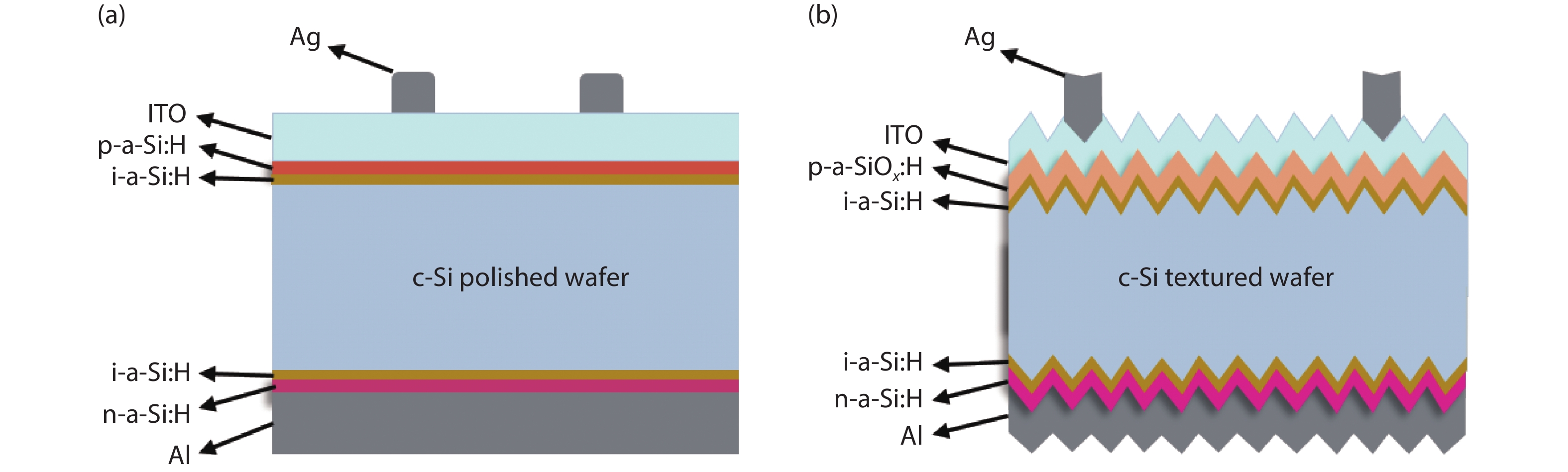
In this study, the EQE spectra of c-Si HIT solar cell[
![]()
Figure 1.(Color online) Structures of (a) flat and (b) textured HIT solar cell in this study.
3. Principle of EQE simulation
3.1. Optical constants obtained by spectroscopy
In this study, the optical constants of each film were obtained by simply measured transmittance and reflectance curves from UV–Vis–NIR spectroscopy. The procedure goes as follows: first, some sets of optical constants among expected wavelength range corresponding to different layers can be acquired from public resources[
The modification process is related to the conclusion that n and k are wavelength-dependent functions, and every function of λ may be expressed by means of an infinite power series[
Here, an, bn, cn, ak, bk, ck… are constants.
According to Eqs. (1) and (2), the difference between the initial data n(λ), k(λ) and the modified data can be expressed by
where Δn(λ) and Δk(λ) represent the difference values and the actual optical constants can then be expressed as n(λ) + Δn(λ) and k(λ) + Δk(λ). The Δan, Δbn, Δcn, Δak, Δbk, Δck… are the main parameters and the main work is to find these parameters in Eq. (3) and Eq. (4) to minimize the following functions:
where Rmeasured and Tmeasured are the measured reflectance and transmittance in a proper wavelength range (such as 300–1200 nm), respectively, and the Rcalculated, Tcalculated represent the corresponding calculated data. The numerical value of the
The method presented above is based on the Cauchy dispersion formula[
We applied this method to ITO, p-a-Si:H, i-a-Si:H and n-a-Si:H based on the reported optical constants of these films[
![]()
Figure 2.(Color online) The fitting results of measured/calculated transmittance and reflectance curves of different layers. (a) ITO. (b) p-a-Si:H. (c) i-a-Si:H. (d) n-a-Si:H.
![]()
Figure 3.(Color online) The calculated results of optical constants of different layers. (a) ITO. (b) p-a-Si:H. (c) i-a-Si:H. (d) n-a-Si:H.
The obtained n, k values of these materials will serve as the usable parameters in the following EQE calculation.
3.2. EQE calculation method
Most solar cells generally consist of transparent conductive oxide (TCO) layers, an active absorption layer and rear contact materials. From an optical point of view, this device can be considered as a multi-layer film system composed of absorption and non-absorption layers[
![]()
Figure 4.(Color online) Schematic optical model of (a) multi-layer system with all coherent layers and (b) multi-layer system with coherent and incoherent layers.
where H and E are the magnetic and electric fields, respectively. The η can also be expressed as η = NY[
Here, ηj and ηs are the optical admittance of the jth layer and the substrate respectively. δj shows the phase thickness expressed as δj = 2πNjdj/λ, here, dj and λ are the thickness of the jth layer and wavelength, respectively.
The reflectance R can then be obtained by[
where n0 is the refractive index of air, which equals to 1. Yeff is the effective optical admittance Yeff of the multi-layer film system which can be expressed as Yeff = C/B
The transmittance T can be obtained by
The absorptance A of the multi-layer film system can thus be written as A = 1 – T– R.
However, this method can only be employed under an coherent condition. For most solar cells, the optical response needs to be calculated under an incoherent condition. Fujiwara et al. have established an optical model in coherent and incoherent multi-layer film systems[
where t is the total number of assumed waves and p is the serial number of each wave (p = 0, 1, 2, …, t – 1). Then the reflectance RCPA in this method can be expressed by[
Here, the Yeff(δj(p)) represents optical admittance of the overall multi-layer system in which the pth wave in the coherent layer were concerned.
The transmittance TCPA can be obtained using Eq. (8)
where the BC*(δj(p)) represents the calculated BC* of the overall multi-layer system in which the pth wave in the coherent layer were concerned, which is shown in Fig. 4(b).
Finally, the absorptance can be determined as follows[
Based on this method, the total absorptance of the flat solar cell can be calculated. When the carrier collection rate is 100%, EQE = A. However, in the actual process, due to the parasitic absorption, carriers cannot be completely collected. Therefore, for a flat solar cell containing an absorbing layer and other functional layers, the EQE can be obtained by[
where Apfront and Apback represent the parasitic absorption of the front and the back layers of the solar cell which can be obtained based on the above optical model, respectively. Since most rear electrodes of the solar cell allow no transmission, such as silver or aluminum, the total A of the device can be expressed as A = 1 – R[
For textured solar cells, Eq. (11) cannot be used because the reflectance is significantly lower in visible light region than that of flat solar cell[
Using the same method as the flat device, the EQE of textured solar cell can also be calculated.
4. Results
4.1. Simulation and analysis of flat HIT solar cell
The actual optical constants of each layer of the flat HIT solar cell were obtained by the above method. For the case of the bulk c-Si, air was used as the substrate. Unfortunately, since 275-μm thick c-Si is not comparable with other layers in thickness value, the result of Yeff will become very large, which is quite difficult to calculate. Therefore, the thickness of c-Si used for calculation must also be decreased to a range that can be calculated by the computer. However, decreasing the thickness will inevitably reduce the absorption of c-Si[
![]()
Figure 5.(Color online) The fitting results of measured/calculated transmittance and reflectance curves on a modified c-Si thickness of 8000 nm with (a)
By applying the modified optical constants of these films into Eq. (7), the characteristic matrix of the device can be obtained, and finally the EQE can be calculated from Eq. (14). Fig. 6(a) shows the comparison between the calculated EQE and the measured EQE of the flat HIT solar cell. It can be seen again that with t = 1 in Eq. (10), the optical interference occurred in the long wavelength region, which would be eliminated in the case of t = 10 in Eq. (10), thus resulted in a remarkable matching between the calculated curves and the experimental data. The integrated current of the cell from the EQE spectra was 35.2 mA/cm2 (measured) and 34.3 mA/cm2 (calculated), respectively. This difference was attributed to the optical response in the short wavelength region, which can be explained by the difference between the thickness of the films measured on glass and the thickness of each layer in the actual device in the calculation process. Figs. 6(b) and 6(c) show EQE spectra with different p-a-Si:H and i-a-Si:H thicknesses, from which we can see that with the thickness of p-a-Si:H or a-Si:H increasing, the EQE data showed distinctly different curves in the short wavelength region[
![]()
Figure 6.(Color online) The calculation results of EQE simulation on the flat HIT solar cells. (a) The fitting results between the measured EQE and different calculated curves. (b) and (c) The EQE sensitivity on the thickness of p-a-Si:H and i-a-Si:H layers, respectively.
Based on an integral process, the optical contribution of each layer of the flat HIT solar cell was further calculated, as shown in Fig. 7. Furthermore, Fig. 7(a) gives an EQE analysis on the device, with different color region corresponding to different optical loss (or gain) of each component layer, while Fig. 7(b) represents a clear numerical summary of the mentioned current contributions. In the short wavelength region, the parasitic absorption of ITO and a-Si:H layers have taken up most of the total absorption, which is an important limiting factor on the short-circuit current density Jsc of the HIT solar cells since the carrier collection here is almost 0[
![]()
Figure 7.(Color online) Optical analysis of the flat HIT solar cell. (a) Measured/calculated EQE results. (b) The contribution of each layer on the current loss (or gain) in the device.
4.2. EQE calculation of HIT with p-a-SiOx:H
To increase the current from short wavelength, an emitter layer of p-a-SiOx:H has been utilized to substitute p-a-Si:H, due to its wider optical band gap[
![]()
Figure 8.(Color online) Calculation results of flat HIT solar cell with p-a-SiO
4.3. EQE calculation of HIT with Ag/Al electrode as rear metal layer
To further evaluate the current improvement in the long wavelength region (> 1000 nm), we utilized Ag/Al to replace Al as the rear metal layer in HIT solar cells[
![]()
Figure 9.(Color online) Calculation results of flat HIT solar cell with Ag/Al electrode as rear metal layer. (a) EQE calculation results. (b) The contribution of each layer on the current loss (or gain) in the device.
4.4. EQE simulation and analysis of textured HIT solar cell
This simulation method for the flat HIT solar cell can also be applied to the textured HIT solar cells. The difference is that the reflectance of the textured solar cell has to be actually measured since the anti-reflection effect of the textured c-Si is difficult to calculate. Based on the REPS, the EQE of the textured HIT solar cell can be calculated from Eq. (15), corresponding optical loss (gains) could be analyzed in the same way as the case in the flat HIT solar cells. It should also be noted that the top angle of pyramid-shaped texture is confirmed to be 80°[
Fig. 10(a) shows the calculated result for a textured HIT solar cell. Again, the calculated curve shows a perfectly matching with the measured data, and the integrated current of the cell from the EQE spectra was 39.2 mA/cm2 (measured) and 39.1 mA/cm2 (calculated), respectively. Fig. 10(b) corresponds to the calculated contribution of each layer on the current loss (or gain) in the device. Compared with the calculated results of the flat solar cell in Fig. 8(b), the overall reflection of the device was decreased by ~70%, accompanied by a preferable increase of ~20% in the absorption of the bulk c-Si, as well as an unavoidable increase in the parasitic absorption of the rear Al layer due to more light trapping in the device.
![]()
Figure 10.(Color online) Optical analysis of the textured HIT solar cell. (a) Measured/calculated EQE calculation results. (b) The contribution of each layer on the current loss (or gain) in the device.
5. Conclusion
We established a spectroscopy-based method to obtain the actual optical constants of the layers in a solar cell device for the optical simulation of EQE. Combined with the measured transmittance and reflectance spectra from UV–Vis–NIR system and some sets of public standard reference data, a modification on optical constants was conducted via simple computational calculation, from which corresponding n, k values can be obtained and served as the actual data in the device. This approach enables us to develop an accurate EQE simulation method. The calculation results show remarkable agreements with the experimental data, both in flat and textured HIT applications. Furthermore, different contributions of each layer on the overall current loss (or gain) have been analyzed. In addition, different promising techniques related to the considerations in different wavelength ranges have been applied to our calculation method. The results show that a doped p-a-SiOx:H layer in the front side can repress ~50% of the parasitic absorption of p-a-Si:H in the short wavelength, while we can expect another reduction of > 60% of the parasitic absorption of Al electrode in the long wavelength region by utilizing Ag/Al as rear metal layers. These routines indicate the practical accuracy and versatility of our EQE simulation approach. Finally, an ongoing study of our calculation method in other photovoltaic devices has been made and will be reported in the future.
Acknowledgement
The authors gratefully acknowledge the supports from National Key Research and Development Program of China (Grant No. 2018YFB1500103), National Natural Science Foundation of China (Grant Nos. 61474065 and 61674084), Tianjin Research Key Program of Science and Technology (Grant No. 18ZXJMTG00220), 111 Project (Grant No. B16027), and Fundamental Research Funds for the Central Universities.
References
[1] K Ding, T Kirchartz, B E Pieters et al. Characterization and simulation of a-Si:H/
[2] M Jošt, E Köhnen, A B Morales-Vilches et al. Textured interfaces in monolithic perovskite/silicon tandem solar cells: advanced light management for improved efficiency and energy yield. Energy Environ Sci, 11, 3511(2018).
[3]
[4] T Hara, T Maekawa, S Minoura et al. Quantitative assessment of optical gain and loss in submicron-textured CuIn1−
[5] A Nakane, H Tampo, M Tamakoshi et al. Quantitative determination of optical and recombination losses in thin-film photovoltaic devices based on external quantum efficiency analysis. J Appl Phys, 120, 064505(2016).
[6] A Nakane, S Fujimoto, H Fujiwara. Fast determination of the current loss mechanisms in textured crystalline Si-based solar cells. J Appl Phys, 122, 203101(2017).
[7] D E Aspnes, A Studna. A high precision scanning ellipsometer. Appl Opt, 14, 220(1975).
[8] G Jakopic, W Papousek. Unified analytical inversion of reflectometric and ellipsometric data of absorbing media. Appl Opt, 39, 2727(2000).
[9] M H Chiu, J Y Lee, D C Su. Complex refractive-index measurement based on Fresnel's equations and the uses of heterodyne interferometry. Appl Opt, 38, 4047(1999).
[10] M H Chiu, J Y Lee, D C Su. Refractive-index measurement based on the effects of total internal reflection and the uses of heterodyne interferometry. Appl Opt, 36, 2936(1997).
[11] Y Y Cheng, J C Wyant. Multiple-wavelength phase-shifting interferometry. Appl Opt, 24, 804(1985).
[12] Y Y Cheng, J C Wyant. Two-wavelength phase shifting interferometry. Appl Opt, 23, 4539(1984).
[13] G Leveque, Y Villachon-Renard. Determination of optical constants of thin film from reflectance spectra. Appl Opt, 29, 3207(1990).
[14] J M Siqueiros, L E Regalado, R Machorro. Determination of (
[15] M F Al-Kuhaili, E E Khawaja, S M Durrani. Determination of the optical constants (
[16] J I Cisneros. Optical characterization of dielectric and semiconductor thin films by use of transmission data. Appl Opt, 37, 5262(1998).
[17] C C Katsidis, D I Siapkas. General transfer-matrix method for optical multilayer systems with coherent, partially coherent, and incoherent interference. Appl Opt, 41, 3978(2002).
[18]
[19] M Taguchi, A Yano, S Tohoda et al. 24.7% record efficiency HIT solar cell on thin silicon wafer. IEEE J Photovolt, 4, 96(2014).
[20]
[21] M Nenkov, T Pencheva. Calculation of thin-film optical constants by transmittance-spectra fitting. J Opt Soc Am A, 15, 1852(1998).
[22] D A Likhachev. Practical method for optical dispersion model selection and parameters variations in scatterometry analysis with variable
[23] Z C Holman, M Filipič, A Descoeudres et al. Infrared light management in high-efficiency silicon heterojunction and rear-passivated solar cells. J Appl Phys, 113, 013107(2013).
[24] Z C Holman, A Descoeudres, L Barraud et al. Current losses at the front of silicon heterojunction solar cells. IEEE J Photovolt, 2, 7(2012).
[25] I Chambouleyron, S Ventura, E Birgin et al. Optical constants and thickness determination of very thin amorphous semiconductor films. J Appl Phys, 92, 3093(2002).
[26] F Zhu, J Singh. Study of the optical properties of amorphous silicon solar cells using admittance analysis. J Non-Cryst Solids, 152, 75(1993).
[27] C W Lin, K P Chen, M C Su et al. Admittance loci design method for multilayer surface plasmon resonance devices. Sens Actuators B, 117, 219(2006).
[28] M Theuring, S Geissendörfer, M Vehse et al. Thin metal layer as transparent electrode in n–i–p amorphous silicon solar cells. EPJ Photovolt, 5, 55205(2014).
[29] G Y Margulis, B E Hardin, I K Ding et al. Parasitic absorption and internal quantum efficiency measurements of solid-state dye sensitized solar cells. Adv Energy Mater, 3, 959(2013).
[30] D Zhang, I A Digdaya, R Santbergen et al. Design and fabrication of a SiO
[31] C Ghica, L C Nistor, V S Teodorescu et al. Laser treatment of plasma-hydrogenated silicon wafers for thin layer exfoliation. J Appl Phys, 109, 063518(2011).
[32] H Wang, X Liu, Z M Zhang. Absorption coefficients of crystalline silicon at wavelengths from 500 nm to 1000 nm. Int J Thermophys, 34, 213(2013).
[33]
[34] K M McPeak, S V Jayanti, S J Kress et al. Plasmonic films can easily be better: rules and recipes. ACS Photonics, 2, 326(2015).
[35] J P Seif, A Descoeudres, M Filipič et al. Amorphous silicon oxide window layers for high-efficiency silicon heterojunction solar cells. J Appl Phys, 115, 024502(2014).
[36] J Sritharathikhun, H Yamamoto, S Miyajima et al. Optimization of amorphous silicon oxide buffer layer for high-efficiency p-type hydrogenated microcrystalline silicon oxide/n-type crystalline silicon heterojunction solar cells. J Appl Phys, 47, 8452(2008).
[37] H Fujiwara, T Kaneko, M Kondo. Application of hydrogenated amorphous silicon oxide layers to c-Si heterojunction solar cells. Appl Phys Lett, 91, 133508(2007).
[38] C Battaglia, S M De Nicolas, S De Wolf et al. Silicon heterojunction solar cell with passivated hole selective MoO
[39] X Zhang, Y Zhao, Y Gao et al. Influence of front electrode and back reflector electrode on the performances of microcrystalline silicon solar cells. J Non-Cryst Solids, 352, 1863(2006).
[40] Z C Holman, A Descoeudres, S D Wolf et al. Record infrared internal quantum efficiency in silicon heterojunction solar cells with dielectric/metal rear reflectors. IEEE J Photovolt, 3, 1243(2013).
[41] K S B D Silva, V J Keast, A Gentle et al. Optical properties and oxidation of α-phase Ag–Al thin films. Nanotechnology, 28, 095202(2017).
[42] N Matsuki, H Fujiwara. Nondestructive characterization of textured a-Si:H/c-Si heterojunction solar cell structures with nanometer-scale a-Si:H and In2O3:Sn layers by spectroscopic ellipsometry. J Appl Phys, 114, 18(2013).
[43] K Watanabe, N Matsuki, H Fujiwara. Ellipsometry Characterization of hydrogenated amorphous silicon layers formed on textured crystalline silicon substrates. Appl Phys Express, 3, 116604(2010).

Set citation alerts for the article
Please enter your email address
© Copyright 2018-2021 | Chinese Laser Press. All Rights Reserved 沪ICP备15018463号-20