
Xu Liu, Yunduo Li, Lianhua Ye, Zhangcheng Huang, Songlei Huang, Jiaxiong Fang. Pixel-level high resolution and low error rate time-to-digital converter circuit of single photon detection InGaAs avalanche focal plane array[J]. Infrared and Laser Engineering, 2021, 50(11): 20210009
- Infrared and Laser Engineering
- Vol. 50, Issue 11, 20210009 (2021)
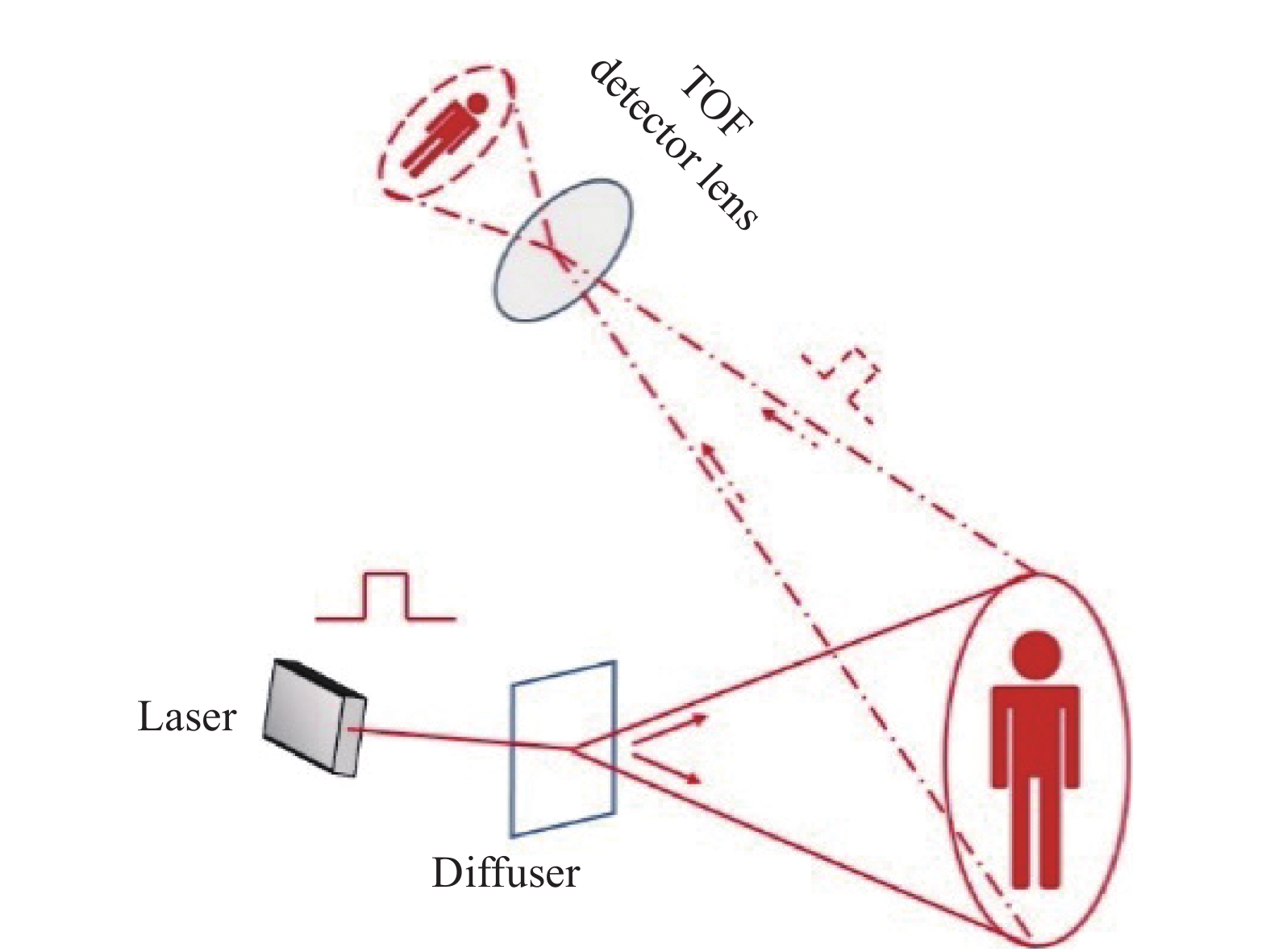
Fig. 1. Working principle of time-to-digital converter circuit
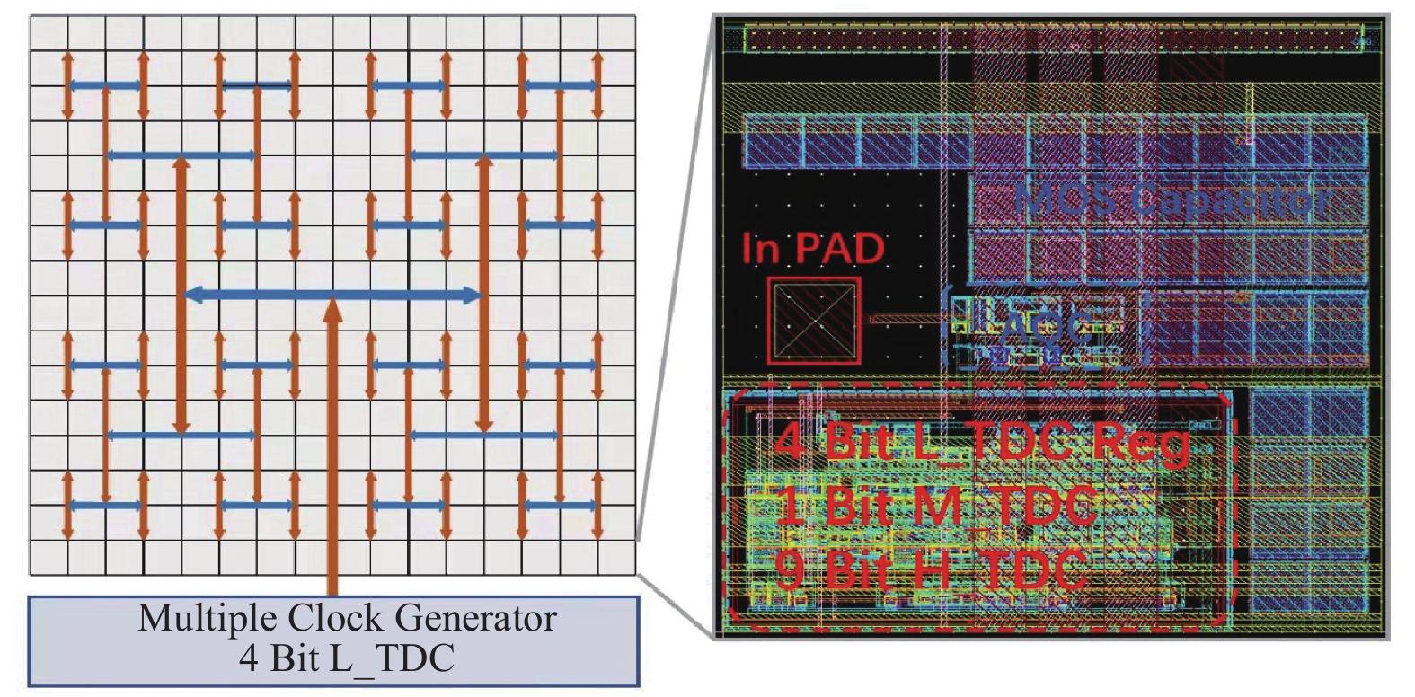
Fig. 2. Structure of three-stage time-to-digital converter circuit
Fig. 3. Working sequence of three-stage time-to-digital converter circuit
Fig. 4. Three-stage time-to-digital converter circuit
Fig. 5. Structure of delay-locked loop circuit
Fig. 6. Voltage-controlled delay chain and delay unit
Fig. 7. Voltage-controlled delay chain - Multi-stage split-phase clock
Fig. 8. Global clock network layout
Fig. 9. Low segment data latch circuit. (a) Data latch circuit before optimization; (b) Data latch circuit after optimization
Fig. 10. Schematic diagram of inter-segment errors
Fig. 11. Delay error of asynchronous counter
Fig. 12. Delayed sampling of M_TDC signal
Fig. 13. High segment - linear feedback shift register
Fig. 14. Microscope photo of array type TDC
Fig. 15. Block diagram of TDC test system
Fig. 16. Time-to-digital conversion curve. (a) Full-scale conversion curve; (b) 1112 ns partial amplification conversion curve
Fig. 17. Statistical distribution of TDC conversion steps
Fig. 18. Differential non-linearity test results
Fig. 19. Integral non-linearity test result
Fig. 20. Non-ideal duty cycle split-phase clock
|
Table 1. Count value of time-to-digital converter circuit
|
Table 2. Conversion step size statistics of time-to-digital converter circuit
|
Table 3. Summary of time-to-digital circuit index


Set citation alerts for the article
Please enter your email address

© Copyright 2018-2021 | Chinese Laser Press. All Rights Reserved 沪ICP备15018463号-20