
Yuechen Jia, Shixiang Wang, Feng Chen. Femtosecond laser direct writing of flexibly configured waveguide geometries in optical crystals: fabrication and application[J]. Opto-Electronic Advances, 2020, 3(10): 190042-1
- Opto-Electronic Advances
- Vol. 3, Issue 10, 190042-1 (2020)
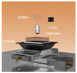
Fig. 1. Schematic illustration of a typical experimental setup for FsLDW operation.
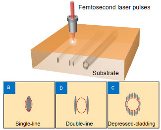
Fig. 2. Schematic illustrations FsLDW of (a ) single-line waveguides based on smooth Type-Ⅰ modification, (b ) stress-induced double-line waveguides based on two parallel Type-Ⅱ laser tracks, and (c ) depressed-cladding waveguides.
Fig. 3. Schematic illustration of nonlinear waveguide channels based on FsLDW single-/multi-line geometries.
Fig. 4. (a ) Schematic illustration of Y-branch waveguide channels based on FsLDW double-line geometry39. (b ) The microscopic photograph of the splitting region in a FsLDW Yb:YAG waveguide splitter39.
(c ) The cross-sectional microscopic photograph of a FsLDW Nd:YAG waveguide array43. (d ) Reconstructed refractive index profile of the fabricated waveguide array43. Scale bars denote 30 µm. Figure reproduced with permission from: (a, b) ref.39 and (c, d) ref.43, Optical Society of America.
Fig. 5. (a ) Schematic illustration of curved waveguide channels based on FsLDW depressed-cladding geometries34. (b ) Schematic illustration of three-element 3D photonic-lattice-like cladding photonic structures for beam splitting and ring-shaped beam transformation31. Figure reproduced with permission from: (a ) ref.34, SPIE; (b) ref.31, Optical Society of America.
Fig. 6. Schematic illustration of a MZI EO modulator with Y-branch waveguide channels based on FsLDW double-line geometries58.
Figure reproduced with permission from ref.58, Optical Society of America.
Fig. 7. (a ) Lasing performance of FsLDW curved Yb:YAG double-line waveguides with different curvature radii R 38. (b–e ) Output modal profiles of FsLDW beam splitters and ring-shaped beam transformers49, 50. Figure reproduced with permission from: (a) ref.38, Optical Society of America; (b, e) ref.49, Springer Nature; (c, d) ref.50, IEEE.
Fig. 8. Modal profiles of SHG (1064→532 nm) and 1×4 beam splitting from photonic-lattice-like KTP cladding waveguides69.
Figure reproduced with permission from ref.69, Springer Nature.
|
Table 1. EO performance of reported FsLDW Y-branch waveguides in crystals.
|
Table 2. Lasing performance of reported FsLDW 3D waveguides in crystals.


Set citation alerts for the article
Please enter your email address

© Copyright 2018-2021 | Chinese Laser Press. All Rights Reserved 沪ICP备15018463号-20