Abstract
Optical waveguides are far more than mere connecting elements in integrated optical systems and circuits. Benefiting from their high optical confinement and miniaturized footprints, waveguide structures established based on crystalline materials, particularly, are opening exciting possibilities and opportunities in photonic chips by facilitating their on-chip integration with different functionalities and highly compact photonic circuits. Femtosecond-laser-direct writing (FsLDW), as a true three-dimensional (3D) micromachining and microfabrication technology, allows rapid prototyping of on-demand waveguide geometries inside transparent materials via localized material modification. The success of FsLDW lies not only in its unsurpassed aptitude for realizing 3D devices but also in its remarkable material-independence that enables cross-platform solutions. This review emphasizes FsLDW fabrication of waveguide structures with 3D layouts in dielectric crystals. Their functionalities as passive and active photonic devices are also demonstrated and discussed.Introduction
Active and passive photonic devices constructed based on dielectric waveguide technology play significant roles in photonic integrated circuits (PICs)1, 2. The great interest in such devices largely stem from the compact geometries of waveguide structures, which allows for optical confinement within extremely compressed volumes of micrometric or sub-micrometric scales, reaching considerably high optical intensities with respect to that in bulk materials. Thus, monolithically integrated optical waveguide devices are expected to prevail against bulk setups for applications in a wide range of research areas3-5. Being compatible simultaneously with robustness and multi-functionality, optical waveguides defined in different dielectric crystals show superior performance in terms of tailoring light properties over that in glassy amorphous host materials as active optical devices such as high-power and low-threshold lasers, high-efficiency nonlinear wavelength converters, and high-speed optical modulators. These intriguing features are primarily attributed to the unique crystal lattice structures6.
Developing practical and flexible fabrication techniques for high-quality waveguide channels in heterogeneous substrates is in any case the primary task. The key concept is to construct a guiding structure composed of a higher-refractive-index core, i.e., a waveguiding core, that is surrounded by lower-refractive-index cladding layers, which could be air or/and unmodified substrate regions. Although a number of refractive-index-contrast creation/modification technologies have been well developed to this end, most of the commonly used approaches, such as epitaxial growth, wafer bonding, ion implantation/ irradiation, and standard photolithography, allow only fabrication of waveguide architectures on/near substrate surfaces3–5, 7, 8. Besides, most of conventional technologies are still restricted to prototyping planar two-dimensional (2D) layouts, thus resulting in optical designs with large dimensions/footprints and high complexity to ensure efficient optical connections. Furthermore, the tedious and multi-step surface structuring/patterning operations for producing on-demand waveguide channels are usually high-cost and full of risks as each engineering step individually impacts the properties of the final waveguide device significantly 9, 10. These bottlenecks can be well overcome by femtosecond laser direct writing (FsLDW), which is a rapidly evolving technology exploiting tightly focused femtosecond laser pulses to modify the optical properties of a small volume inside a transparent material, inducing localized and controllable refractive index modification in a direct procedure without using any patterned masking11, 12. Such technology therefore allows monolithic and sophisticated waveguide fabrication in a very flexible manner. In addition, FsLDW exhibits good compatibility with a broad range of crystal families providing a promising avenue for constructing multifunctional optical devices towards 3D integrated photonics13, 14.
Several review articles on FsLDW of dielectric materials in general have been published12, 14. A further article concentrating on FsLDW of 3D integrated photonics based on only glasses has also been published15. In contrast to that of glasses, fabrication of 3D photonic devices in dielectric crystals employing FsLDW is more challenging due to the complexity in crystal lattice structures. In the past decade, however, regardless of the aforementioned challenges, the research field of FsLDW 3D crystalline photonic devices has experienced tremendous growth, leading to a number of optical functions realized in bulk-like waveguide-based devices. Therefore in this article, recent advances in 3D photonic devices based on FsLDW crystalline waveguides are reviewed. Following the Introduction, the next section is devoted to describing the fundamentals of femtosecond laser induced modifications in dielectric crystals, and then discussing the evolved design prototypes based on these structural modifications for constructing 3D waveguide geometries. The Photonic applications section summarizes experimental demonstrations of crystalline waveguides with nonlinear geometries, concentrating on their characteristics as active optical components. Finally, this review article concludes with a brief summary and perspectives for potential future directions.
Femtosecond laser direct writing of crystalline waveguides
As a "newly" discovered 3D micromachining and microfabrication technology, femtosecond laser micromachining immediately delivered both enhanced performance and simplicity in use in the study of compact and channelized waveguide architectures in transparent dielectrics since the pioneering work of Davis et al. in 199616, winning an increasingly significant place in micro-/nano-fabrication and simultaneously and opening up new opportunities for multidisciplinary fields11-15. The great interest of using tightly focused femtosecond laser pulses, instead of longer pulses (e.g., nanosecond and picosecond) and other conventional approaches, for high-precision material micromachining is that micro-/nano-modifications can be realized in a very small region of the target substrate on a timescale much shorter than the thermal energy exchange between photo-excited electrons and lattice ions, enabling smooth photo-modifications with extremely high spatial resolution11.
The laser-induced localized modification that occurs in dielectric crystals strongly relies on the nonlinear-optical absorption of the incident laser pulses, which triggers the structural damages of the material. Two classes of nonlinear excitation mechanisms, namely nonlinear photoionization and avalanche ionization, play important roles in this nonlinear laser-matter interaction process11. When a sufficient amount of energy is absorbed via these two mechanisms and is deposited into the material via electron-phonon coupling and defect formation, permanent damage occurs. There is no widely accepted definition of a damage threshold, but in order to excite a significant number of free electrons, a laser intensity in the range of 1012–1013 W/cm2 is usually required12. It is well accepted that the laser-induced plasma is the origin of the modifications that will take place at the focal volume after the laser-matter interaction process11, 12. However, physical mechanisms and dynamics that take place after the free-electron plasma has transferred its energy to the crystal lattice, are not fully understood yet11, 12.
Flexibility - a real 3D micromachining technology
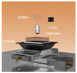
A typical experimental setup for FsLDW in dielectric crystals is schematically illustrated in Fig. 1. In the laser micromachining operation, the sample is usually placed on a computer-controlled XYZ-motorized translation stage for 3D motion with respect to the beam focal spot, and the laser beam is in general fixed and focused at a certain depth beneath the sample surface via a set of focusing lenses. The sample can be translated either parallel to the laser beam, i.e., longitudinal writing scheme, or perpendicular, i.e., transverse writing scheme. The waveguide structures fabricated by using the former method possess circular cross sections with good symmetry, but the longitudinal writing depth is limited by the working distance of the focusing lens and spherical aberrations, which usually distort the focus11. Such scheme is therefore not often used for constructing nonlinear waveguide geometries with 3D layouts. In contrast, the transverse geometry, which can abandon the constraints of the lens working distance, allows implementation of more complex structures with flexible configurations and unrestricted dimensions, in spite of their asymmetric droplet-shape cross sections11, 12. Yet, the waveguide symmetry can still be accessible with transverse scanning by further employing multi-scan strategy and beam reshaping techniques, or simply introducing waveguides with step-index profiles11.

Figure 1.Schematic illustration of a typical experimental setup for FsLDW operation.
Diversity - linear waveguide geometries
The observed structural modifications in crystalline materials induced by focused femtosecond lasers can be mainly categorized into two types depending on whether the working intensity of the laser pulses exceeds the optical damage threshold of the target material or not17. In case of a low-intensity laser irradiation, i.e., the so-called weak damage regime (Type-Ⅰ modification, below the optical damage threshold), a smooth refractive index change at the focal volume is formed. In contrast, for high peak intensity, severe damages (Type-Ⅱ modification) with localized defect formation and material network rearrangement are produced. The sign of the refractive index change strongly depends on the modification mechanisms, or more fundamentally, on the laser exposure conditions (focusing conditions, pulse energy, repetition rate, pulse duration, etc.) and the physical properties (bandgap, dispersion, ionization rates, thermal conductivity, etc.) of the target materials11, 12. The most commonly used morphological geometries of waveguides in dielectric crystals are characterized as tunnel-like "single-line" (based on Type-Ⅰ modification), stress-field induced "double-line" (based on Type-Ⅱ modification), and fiber-like "depressed-cladding" (based on Type-Ⅱ modification) structures. The cross-sectional illustrations of these waveguide configurations are shown in Fig. 2.
Figure 2.Schematic illustrations FsLDW of (a) single-line waveguides based on smooth Type-Ⅰ modification, (b) stress-induced double-line waveguides based on two parallel Type-Ⅱ laser tracks, and (c) depressed-cladding waveguides.
In a single-line waveguide configuration, highly focused laser will induce positive refractive-index changes (∆n > 0) at the irradiated focal volume, where the guiding core is eventually located. This positive change mechanism is very common in amorphous materials, e.g., in a majority of glasses. Such feature enables direct writing of 3D guiding structures with flexible geometries for easy construction of passive devices, such as splitters, directional couplers, and waveguide arrays/gratings, by simply scanning the target sample along arbitrary directions11, 15, 18. In crystals, however, such mechanism seems to be hampered by the periodic lattice structures and so far it has been only realized in a handful of hosts, e.g., LiNbO3, ZnSe, YCa4O(BO3)3 (YCOB), and Bi4Ge3O12 (BGO)12, 19-23. Even in these crystals, single-line waveguides still suffer from serious polarization-dependent guiding, bulk-related property degradation, and poor thermal stability, which limit the practical applications of such waveguides in crystals for high-performance active photonic devices significantly12. Nevertheless, because of its simplicity and flexibility in fabrication, such single-line structures still have research values, provided that the target bulk features can be maintained to an acceptable level, for enabling a very convenient way for direct fabrication of 3D waveguide structures.
As for the double-line waveguide configuration, the focused femtosecond laser causes localized crystalline lattice expansion in the focal volume, which could induce negative refractive-index changes (∆n < 0) in the directly irradiated regions12. Consequently, the vicinal regions may possess a relatively high index because of the stress-induced effects. Usually, if there are two parallel laser tracks with suitable separation (typically 10–20 µm), the waveguide core is located in between, forming a double-line waveguide12, 19. In contrast to the single-line structures, double-line waveguides have considerable advantages in terms of wide applicability of crystalline materials, good preservation of original bulk-related features, better controllability on refractive-index profiles, and superior thermal stability12, 20. However, since the waveguide core of such structure is not at the laser-written region, special designs are usually needed for double-line geometries towards the fabrication of 3D waveguide structures, which is prone to introduce roughness and thus larger scattering losses. In addition, such waveguides still suffer from the polarization-dependent guiding as the single-line ones, which makes the realization of some nonlinear optical devices challenging, e.g., nonlinear optical frequency converters which require excellent guidance along orthogonal polarizations12. In general, the maximum ∆n induced by FsLDW Type-Ⅰ modification is much lower than that of Type-Ⅱ modification at the laser tracks. For example, the maximum ∆n of a Type-Ⅰ-based single-line LiNbO3 waveguide is generally < 10-3, while this value will increase to around ~5 × 10⁻³ level at the directly irradiated tracks in case of a Type-Ⅱ-based double-line structure to support a valid waveguiding19, 20. In case of Nd:YAG double-line waveguides, ∆n as high as 9 × 10⁻² at the Type-Ⅱ laser filaments has been determined according to μ-Raman and μ-photoluminescence microscopic analysis24. Detailed discussion on FsLDW-induced refractive index changes, localized lattice modifications, and the corresponding waveguide simulation/modeling approaches can be found in Refs.24-26.
A depressed-cladding waveguide is consisted of a guiding core surrounded by a number of low-index laser tracks. Those laser tracks are close to each other (few micrometers), constructing a quasi-continuous low-index potential barrier, providing the required optical confinement12, 27. Theoretically, laser tracks can be arranged flexibly to produce waveguide structures with cross sections of arbitrary geometries28. In practice, a circular shape is preferred because it fits well to the optical fibers. Besides, cladding structures are proven to be able to support adjustable modal profiles including fundamental and high-order modes in an individual waveguide29, 30. Therefore, optimal optical coupling and fine connection for flexible fiber-waveguide-fiber networks can be expected. Since the guiding core in such structures is again located at regions beyond the reach of the laser-induced damages, most of the advantages that double-line waveguides possess also apply to cladding waveguides. Furthermore, the greatest interest in such cladding structures is its unique 2D-guidance feature, which means that the circular cladding waveguide usually features almost identical guiding properties along different excitation polarizations12. This makes it an ideal platform for unpolarized pumping as laser source and nonlinear optical frequency converter. However, since its relative complexity in fabrication and usually large-size in their layouts, curved or/and branched cladding waveguide fabrications are quite challenging and time-consuming.
Variability - design prototypes for nonlinear waveguide geometries
All three kinds of FsLDW waveguide geometries introduced in "Diversity - linear waveguide geometries" Section are usually in straight, i.e., 2D, channel layouts, forming conventional linear waveguides. While, in many more cases for on-chip photonic applications in integrated optics, curved, or to say nonlinear, waveguide channels are more favorable1. Therefore, a lot of efforts have been made on exploring new design prototypes based on the commonly-used linear waveguide geometries towards the construction of 3D optical components31. In this section, these newly evolved design prototypes are overviewed.
Due to its simplicity in fabrication, single-line waveguides are the early research focuses of FsLDW linear and nonlinear waveguide geometries, especially based on multi-functional LiNbO3 crystals 20, 32. Recently, 1×4 beam splitters and ring-shape distributed beam profiles have been demonstrated based on single-line waveguides in LiNbO333 and BGO34, respectively. Furthermore, a variant evolved from single-line approach carries out multiple laser scans that are overlapped/neighbored transversally to the writing direction. This is the so-called multipass technique35, which can be used to construct positive step-index cores with configurable, e.g., symmetric, cross-sectional shapes and even tailored modal profiles36. This approach also offers the possibility to fabricate a waveguide supporting guidance at longer wavelengths since the guiding core in this case is larger than a single-line structure. Figure 3 illustrates the design prototypes of nonlinear waveguide geometries based on the aforementioned single-/multi-line techniques. Such Type-Ⅰ-based structures, however, are susceptible to the thermal deterioration. For example, it has been found that thermal treatment of single-line LiNbO3 waveguides up to only 150 ℃ would significantly degrade their waveguiding properties35 and even completely erase the laser-induced modifications37. This feature is very detrimental to the functionality of high-power or thermal-related optical devices35.
Figure 3.Schematic illustration of nonlinear waveguide channels based on FsLDW single-/multi-line geometries.
In contrast to Type-Ⅰ-based waveguides, Type-Ⅱ-based waveguides generally show better thermal stability and excellent preservation of original optical properties. Although it is not simple, curved and branched waveguide channels have been fabricated based on double-line geometries in crystals38-41, as schematically illustrated in Fig. 4(a). Moreover, by defining a specially designed section (as shown in Fig. 4(b)) within the beam-splitting structure, a variable splitting ratio of two waveguide channels can be realized39. In such a curved waveguide, it has been reported that the effective refractive index is increased towards the outer part of the curve, resulting in mode shift and deformation that might lead to additional mode-mismatch losses at the transition section38. A multi-channel configuration evolved from individual double-line structure is 1D planar waveguide array, which usually consists of multiple double-line waveguides lining up and distributed uniformly with a fixed separation (an arbitrary distribution is also possible)42, 43. A cross-sectional microscopic photograph of such design is shown in Fig. 4(c). In this case, evanescent coupling between two neighboring waveguides is possible because of the tightly bordered waveguide cores, as suggested by the reconstructed refractive index profile in Fig. 4(d). However, since good-quality double-line waveguides with strong optical confinement would largely suppress the evanescent field, efficient evanescent coupling can only be possible with sufficiently weak confinement which leads to enlarged waveguide loss42, 43. Despite their thermal stability, waveguides based on double-line geometries usually suffer from polarization-dependent guiding properties, which is the major roadblock for their practical applications in nonlinear optics12.
Figure 4.(a) Schematic illustration of Y-branch waveguide channels based on FsLDW double-line geometry39. (b) The microscopic photograph of the splitting region in a FsLDW Yb:YAG waveguide splitter39.
(c) The cross-sectional microscopic photograph of a FsLDW Nd:YAG waveguide array43. (d) Reconstructed refractive index profile of the fabricated waveguide array43. Scale bars denote 30 µm. Figure reproduced with permission from: (a, b) ref.39 and (c, d) ref.43, Optical Society of America.
Despite of their complexity in fabrication, depressed-cladding waveguides feature excellent robustness and polarization-independent guiding properties when compared to Type-Ⅰ-based single-line and Type-Ⅱ-based double-line waveguides. By carefully designing the path of each single laser scan, curved cladding structures, which are composed of a group of circularly distributed curved tracks, can be fabricated, as schematically illustrated in Fig. 5(a)34. With such configuration, however, it is still quite challenging to realize branched waveguide channels44-48. To this end, a new family of hexagonal "photonic-lattice-like" cladding photonic structures, which usually contain multiple linear FsLDW tracks (based on Type-Ⅱ modification) periodically packed in a hexagonal layout with cores located at enclosed track-free regions, was proposed49, 50. Due to the ease in arranging and engineering the periodically arrayed laser tracks, tailored 3D beam steering, such as beam splitting and beam transformation, can be easily realized by introducing additional Type-Ⅱ-based laser tracks at certain positions, as schematically illustrated in Fig. 5(b)31. These laser tracks serve as either beam blockers or confiners that reshape the intensity profile of the propagating guided field over a gradually varied or a multi-element assembled configuration. At the expense of more complicated designs and longer fabrication time, photonic-lattice-like cladding waveguides exhibit a designable feature for beam manipulation in a 3D manner, which paves a way to construct compact optical devices based on a wide range of optical crystals51-56. Furthermore, it has been found that the amount of the track lattice layers is an important factor for light field restriction: multi-layer track lattice offers better light confinement than a single-layer structure49. Recently, a single-scan scheme for depressed cladding waveguides in crystals is proposed by using an engineered femtosecond laser with a longitudinally oriented discrete ring-shaped focal intensity profile57. Such a beam profile is generated by employing a special phase mask, by which the fabrication time can be significantly shortened.
Figure 5.(a) Schematic illustration of curved waveguide channels based on FsLDW depressed-cladding geometries34. (b) Schematic illustration of three-element 3D photonic-lattice-like cladding photonic structures for beam splitting and ring-shaped beam transformation31. Figure reproduced with permission from: (a) ref.34, SPIE; (b) ref.31, Optical Society of America.
Alternatively, femtosecond laser micromachining can be properly combined with other waveguide fabrication technology in a flexible way to exploit the advantages of different methods to the full. For example, on the basis of ion-implanted planar waveguides, ridge structures can be defined by using femtosecond laser ablation, which has been used for fabrication of curved and branched ridge waveguides on the substrate surfaces12, 20, 58, 59. Likewise, the optical barriers for providing vertical light confinement can be also provided by FsLDW induced low-index tracks. Together with the laser ablated grooves, surface ridge waveguide splitters in LiNbO3 have been demonstrated60. Most recently, by combining chemical etching with femtosecond laser micromachining, the etching rate of nanopore lattices in YAG and sapphire can be enhanced by more than five orders of magnitude, enabling rapid definition of arbitrary 3D nanostructures with size of 100 nm in crystals61.
Photonic applications
Femtosecond laser micromachined waveguides with nonlinear geometries, i.e., 3D layouts, in crystals can be used in a broad range of active photonic applications. Selected topics of these applications are summarized in this section.
Electro-optic modulators
Electro-optic (EO) modulators are designed to modulate the phase or the intensity (amplitude) of light propagating through them2. Waveguide-based EO modulators are often composed of two branched waveguide channels operating in a Mach-Zehnder interferometer (MZI) configuration, and are critical optical components for multifunctional PICs62. Clearly, such configuration requires waveguides with curved/branched geometries, which is also the first issue that early studies of FsLDW 3D crystalline waveguides focused on20. In a Type-Ⅰ-based single-line LiNbO3 (x-cut) waveguide, the effective EO coefficient (r33) in the waveguide regions has been found to be only half of the original value in the bulk, suggesting degraded EO behavior induced mainly by FsLDW Type-Ⅰ modifications63. Therefore, demonstrations of EO modulators with FsLDW LiNbO3 waveguides so far are mostly based on Type-Ⅱ-based double-line geometries (in which the original optical properties can be well preserved within waveguide volume), as summarized in Table 1. They have metal electrodes either coated on the substrate surfaces64, 65 or embedded in femtosecond laser ablated grooves58, as schematically illustrated in Fig. 6. The waveguide losses, including propagation and bending losses, of these Y-branch waveguides are determined to be as low as 1 dB/cm58. These devices are able to provide extinction ratios (ERs) of 9 dB (with a half-wave voltage Vπ of 19 V) at a wavelength of λ = 632.8 nm, 11 dB (Vπ of 23 V) at 532 nm, and 11 dB (Vπ of 45 V) at 1.55 μm58, 64, 65, , exhibiting unsatisfied performance when comparing to the commercially available LiNbO3 waveguide EO modulators as a result of the non-optimized EO overlap and the high bending losses. It is indeed very difficult to achieve a strong microwave and optical field overlap because the FsLDW waveguides are generally buried inside the substrate, giving relatively limited accessibility to the electrodes and thus to the applied electric field. For the future work on this topic, therefore, much effort is required on the appropriate design of the waveguides-electrodes configurations and the optimization of microwave-optical group velocity matching without sacrificing EO overlap. Nevertheless, it is worth noting that, in refs.20, 64, a 532 nm light source, which is based on the second-harmonic generation (SHG) of 1064→532 nm from a periodically-poled z-cut LiNbO3 (PPLN) double-line waveguide deployed in the straight channel section, combined with the Y-branch MZI EO modulator on the same monolithic chip is demonstrated, achieving an ER of 7 dB but deviated modulation curves64.
| Crystal | Waveguide | Branch angle | Loss | ER (dB) | Vπ (V) | λ |
| LiNbO3
(x-cut)58 | Double-line | 1.2° | 1 dB/cm | 9 | 19 | 632.8 nm |
| LiNbO3
(x-cut)64 | Double-line | 1.5° | 4 dB | 11 | 23 | 532 nm |
| LiNbO3
(x-cut)65 | Double-line | 0.5° | 30 dB | 11 | 45 | 1550 nm |
Table 1. EO performance of reported FsLDW Y-branch waveguides in crystals.
Figure 6.Schematic illustration of a MZI EO modulator with Y-branch waveguide channels based on FsLDW double-line geometries58.
Figure reproduced with permission from ref.58, Optical Society of America.
Compact lasers
In contrast to EO modulators, FsLDW technology of linear/nonlinear geometries in waveguide laser, as implied by the quantity of publications over the last years5, 12, show rich diversity in terms of available crystal families, waveguide layouts, and configuration complexity. Generally, in optical structures with curved and branched geometries, efficient optical feedback for lasing oscillation cannot be achieved due to the non-straight optical channels. However, benefiting from the excellent optical confinement and compressed mode volume, waveguide lasers (including also nonlinear waveguides) feature reduced lasing threshold and enhanced optical gain, partly offsetting the bending effect. Moreover, if the optical gain is sufficiently high, an individual single-pass may also result in efficient lasing oscillation, even without using any reflective coatings or mirrors5, 30.
So far, efficient compact lasers operating both in the continuous-wave (CW) and Q-switched regimes have been successfully demonstrated in FsLDW 3D waveguides based on double-line, 1D planar array, depressed-cladding, and photonic-lattice-like cladding prototypes, as summarized in Table 2. The most commonly used substrates are rare-earth-doped YAG, partly due to its excellent fluorescent, physical and thermal properties. Moreover, it is also possible to realize efficient lasing just by a single-pass optical pumping in for example Yb:YAG which has relatively high optical gain in comparison to other gain media38, 39. This may be a certain extent help to mitigate the negative impacts of inefficient optical feedback, induced by the curved waveguide cavities, imposed on the lasing performance. Nevertheless, FsLDW-based nonlinear waveguide geometries show comparable lasing performance to their straight linear counterparts, as suggested by the results summarized in Table 2. Some detailed noticeable features of these waveguides are summarized as follows:
| Crystal | Waveguide | Operation mode | Loss | Lasing threshold | Slope efficiency |
| Yb:YAG38 | S-shape double-line | CW | 0.8 dB | < 220 mW | 60% |
| Yb:YAG39 | Y-branch double-line | CW | 3.1 dB | 271 mW | 40% |
| Nd:YAG43 | Planar double-line array | CW | 3.7 dB | 70.7 mW | 37% |
| Nd:YAG49 | Photonic-lattice-like cladding | CW & Q-switched | 0.7 dB | ~200 mW | 32% |
| Nd:YAG50 | Photonic-lattice-like cladding | CW | 0.5 dB | ~90 mW | 34% |
| Nd:YAG67 | Y-branch cladding | Q-switched | 1.1 dB/cm | ~450 mW | - |
| Nd:YAG68 | Y-branch cladding | CW | 1.1 dB/cm | 90 mW | 22.4% |
Table 2. Lasing performance of reported FsLDW 3D waveguides in crystals.
A. The FsLDW prototyped curved sections do not introduce much bending losses if the bending curvature is acceptably small. For example, in studies38, 39, 49, 50, the fabricated non-straight waveguides feature lasing thresholds almost the same as that of the reference straight waveguides, suggesting that only minor or even no additional bending losses are introduced to the total losses according to the modified Caird analysis68. As a consequence, lasing oscillation can be realized even without any reflective mirrors in nonlinear waveguides38, 39. In this case, however, the curved part has to be sufficiently long and the curvature has to be sufficiently small. For example, the curvature radius has to be > 20 mm to maintain a good lasing performance in a curved Yb:YAG waveguide, as indicated in Fig. 7(a)38.
Figure 7.(a) Lasing performance of FsLDW curved Yb:YAG double-line waveguides with different curvature radii R38. (b–e) Output modal profiles of FsLDW beam splitters and ring-shaped beam transformers49, 50. Figure reproduced with permission from: (a) ref.38, Optical Society of America; (b, e) ref.49, Springer Nature; (c, d) ref.50, IEEE.
B. Benefiting from the low lasing thresholds, a number of different passive functionalities, including Y-branch splitting39, 66, 1×2 (Figs. 7(b) and 7(c)) and 1×4 beam splitting (Fig. 7(d))49, 50, ring-shaped beam transformation (Fig. 7(e))49, and adjustable discrete diffraction patterns43, have been respectively demonstrated without influencing the active lasing performance too much. By further integrating 2D layered materials as saturable absorbers to the nonlinear waveguides, passively Q-switched pulsed laser operation based on both direct- and evanescent-field interaction configurations have been realized5, 49, 50, 66, further enriching the functionalities and opening up more possibilities of such a compact platform for PICs.
C. Even with close lasing thresholds, the lasing performance of nonlinear waveguides are still 20%–30% worse than that of straight waveguides in terms of slope efficiencies and output powers, as also indicated by the results in Fig. 7(a)38, 39, 49, 50. This is mainly attributed to the distortion/redistribution of guided optical mode/intensity and the weakened mode matching between pump and lasing modes at non-straight regions38, 39. This phenomenon can be further confirmed by slightly changing the pump positions, which leads to a deformation and/or a shift of the optical field at the junction section and results in a redistribution of pump power and thus a change of the splitting ratio for the waveguide channels39.
D. Apart from the lasing characteristics summarized in Table 2, the maximum lasing output power from nonlinear waveguide geometries reported so far reaches 2.29 W under CW operation39. While in Q-switched operation, laser pulses with a repetition rate as high as 4 MHz and a duration as short as 70 ns have been delivered49. These results are comparable to that of FsLDW straight waveguides5, suggesting excellent practicability and feasibility of FsLDW for prototyping compact sources with configurable geometries.
E. There is not many demonstrations on high-power waveguide lasers with Type-Ⅰ-based 3D structures, partly due to their poor thermal stability issues. In contrast, Type-Ⅱ-based curved waveguide structures show much better thermal performance. For Yb:YAG waveguide beam-splitter lasers, it is observed that the output power does not increase linearly anymore when pump powers > 3.73 W, indicating thermal effects because no cooling setup is used therein39. Additionally, the onset of thermal effects is observed strongly depending on the splitting ratio, or to say curvature, of the waveguide splitter, resulting in a better thermal stability for the relatively-low-curvature structure39.
Frequency doublers
Similar to waveguide lasers, waveguide-based frequency converters are capable of exhibiting superior performance over their bulk counterparts since the beam divergence in waveguides is effectively removed, and the high optical intensities as well as mode profiles can be maintained over a long distance. Therefore, the interaction between fundamental and nonlinear polarization waves are boosted1, 2. In FsLDW-based waveguides, frequency conversion processes, mainly SHG, have been demonstrated in a wide range of nonlinear optical crystals12. A precondition to achieve efficient SHG is to fulfill phase-matching condition, which requires the used χ(2) nonlinear optical crystals to be cut along a specific orientation, i.e., birefringence phase matching (BPM), or to possess periodically oriented ferroelectric domains, i.e., quasi phase matching (QPM)2. This argument also applies to 3D waveguides. So far, only photonic-lattice-like cladding waveguides have been successfully demonstrated for efficient SHG in FsLDW-based nonlinear waveguide geometries69. This is mainly because the cladding waveguides feature excellent polarization-independent light guidance, enabling effective BPM for SHG and potentially other nonlinear optical frequency conversion processes12. As a result, based on KTP photonic-lattice-like cladding waveguides, BMP-based SHG (1064→532 nm) and simultaneously 1×4 beam splitting have been demonstrated, delivering green lasers with an output power of 0.65 mW and a conversion efficiency of 14.3%/W, as shown in Fig. 869. The latter value is much larger than the previously reported SHG from KTP waveguides based on other geometries, which is a result of the excellent preservation as well as enhancement of nonlinear optical properties in such a photonic-lattice-like structure. Particularly, the additional losses introduced by the 3D splitters are determined to be only at 0.1 dB level, suggesting good compatibility of photonic-lattice-like cladding structures69.
Figure 8.Modal profiles of SHG (1064→532 nm) and 1×4 beam splitting from photonic-lattice-like KTP cladding waveguides69.
Figure reproduced with permission from ref.69, Springer Nature.
Conclusion and outlook
In this review article, recent advances in FsLDW of 3D crystalline waveguides in terms of fabrication techniques, design prototypes, and active/passive photonic applications have been summarized. By direct fabrication and flexible configuration of monolithic and/or hybrid waveguide-based optical components with 3D layouts in a wide spectrum of optical crystals, enhanced and mixed optical functionalities including beam splitting, beam tailoring, EO modulation, waveguide lasing, and nonlinear optical frequency conversion can be incorporated in a monolithic crystalline platform. These functionalities can be easily integrated with novel optical materials, e.g., 2D layered materials and optical nanostructures3-5, opening up exciting possibilities and opportunities for future complex and multifunctional PICs.
Despite remarkable achievements have been made in FsLDW of 3D waveguide devices in the past decade, there is still room for improvement in their diversity and practicability. For example, the active photonic devices demonstrated so far are still limited to a handful of optical crystals, such as LiNbO3, YAG, and KTP, and optical functionalities, such as EO modulation, lasers, and frequency doublers, as summarized in Section 3. Therefore, to meet the needs of future multi-functional photonic systems integrating complex and hybrid optical elements on a monolithic chip platform, femtosecond laser micromachining of diverse crystalline waveguide devices and novel waveguide concepts are expected to open new opportunities in integrated photonics. A typical example is femtosecond laser micromachining of high-Q whispering gallery resonators, which has been recently proved feasible based on the highly promising lithium niobate on insulator (LNOI) thin film platform70, 71, providing high-performance guided-wave-based optical elements for photonic chips operating in both classical and quantum systems72. In addition, some immediate areas of research focus in photonics may find optimized solutions by employing FsLDW of crystalline waveguides with 3D layouts. For example, rare-earth-doped crystals, which are already widely known as promising candidates for optical quantum memories and qubits, are expected to be excellent systems for on-chip quantum storage devices. Recently, an integrated platform for quantum light storage has been demonstrated in a Type-Ⅰ-based Pr:Y2SiO5 waveguide fabricated by FsLDW73. By further combining with 3D waveguide structures in future work, high spatial multiplexing with matrices of interconnected quantum memory system in a monolithic chip can be expected. Moreover, the demonstrated FsLDW based 3D waveguide devices so far are mostly operating at the near-infrared wavelengths, it is therefore also necessary to further expand the working wavelength band more into, for example, the visible and the mid-infrared ranges by employing diverse substrate crystals3–5, 74.
As a more straightforward strategy, one may reference FsLDW-based 3D waveguide devices in glasses and exploit their potentialities in optical crystals. For example, the lantern waveguide, a multimode waveguide device consisting of a set of identical single-mode waveguide cores and being capable of smooth conversion of beam-smeared incoherent light into single-mode propagation, can be constructed by FsLDW of array waveguide gratings or photonic-lattice-like structures in glasses and, in principle but not yet demonstrated, diverse optical crystals15, 75. Such 3D photonic lantern allows efficient light coupling/propagation and a large number of inputs, and is therefore highly promising in future astronomical applications, i.e., the rising astrophotonics76.
Briefly, in the quest to approach the ultimate level of on-chip integration in robust and compact packages via exploiting FsLDW waveguide technology, besides constantly digging fundamental laser-matter damage mechanisms as well as optimizing fabrication parameters and integration techniques, research efforts should also be put in further exploring emerging/potential photonic functionalities and systems.
Acknowledgements
We are grateful for the financial support from National Natural Science Foundation of China (No. 61775120). Y. Jia acknowledges the support from “Taishan Scholars Youth Expert Program” of Shandong Province and “Qilu Young Scholar Program” of Shandong University, China.
Author contributions
Y. Jia prepared the manuscript, and all authors discussed the results and contributed to the final manuscript.
Competing interests
The authors declare no competing financial interests.
References
[1] G Lifante. Integrated Photonics: Fundamentals(2003).
[2] B E A Saleh, M C Teich. Fundamentals of Photonics(2019).
[3] C Grivas. Optically pumped planar waveguide lasers, Part Ⅰ: Fundamentals and fabrication techniques. Prog Quant Electron, 35, 159-239(2011).
[4] C Grivas. Optically pumped planar waveguide lasers: Part ò: Gain media, laser systems, and applications. Prog Quant Electron, 45-46, 3-160(2016).
[5] Y C Jia, F Chen. Compact solid-state waveguide lasers operating in the pulsed regime: a review[Invited]. Chin Opt Lett, 17, 012302(2019).
[6] D N Nikogosyan. Nonlinear Optical Crystals: A Complete Survey(2005).
[7] J I Mackenzie. Dielectric solid-state planar waveguide lasers: a review. IEEE J Sel Top Quantum Electron, 13, 626-637(2007).
[8] F Chen. Micro- and submicrometric waveguiding structures in optical crystals produced by ion beams for photonic applications. Laser Photonics Rev, 6, 622-640(2012).
[9] M Zhang, C Wang, R Cheng, A Shams-Ansari, M Lončar. Monolithic ultra-high-Q lithium niobate microring resonator. Optica, 4, 1536-1537(2017).
[10] R Wolf, Y C Jia, S Bonaus, C S Werner, S J Herr et al. Quasi-phase-matched nonlinear optical frequency conversion in on-chip whispering galleries. Optica, 5, 872-875(2018).
[11] R Osellame, G Cerullo, R Ramponi. Femtosecond Laser Micromachining: Photonic and Microfluidic Devices in Transparent Materials (Springer, Berlin Heidelberg, 2012)(2012).
[12] F Chen, de Aldana J R Vázquez. Optical waveguides in crystalline dielectric materials produced by femtosecond-laser micromachining. Laser Photonics Rev, 8, 251-275(2014).
[13] K Sugioka, Y Cheng. Femtosecond Laser 3D Micromachining for Microfluidic and Optofluidic Applications(2014).
[14] D Choudhury, J R Macdonald, A K Kar. Ultrafast laser inscription: perspectives on future integrated applications. Laser Photonics Rev, 8, 827-846(2014).
[15] S Gross, M J Withford. Ultrafast-laser-inscribed 3D integrated photonics: challenges and emerging applications. Nanophotonics, 4, 332-352(2015).
[16] K M Davis, K Miura, N Sugimoto, K Hirao. Writing waveguides in glass with a femtosecond laser. Opt Lett, 21, 1729-1731(1996).
[17] S Gross, M Dubov, M J Withford. On the use of the Type Ⅰ and ò scheme for classifying ultrafast laser direct-write photonics. Opt Express, 23, 7767-7770(2015).
[18] M Ams, P Dekker, S Gross, M J Withford. Fabricating waveguide Bragg gratings (WBGs) in bulk materials using ultrashort laser pulses. Nanophotonics, 6, 743-763(2017).
[19] J Burghoff, S Nolte, A Tünnermann. Origins of waveguiding in femtosecond laser-structured LiNbO3. Appl Phys A, 89, 127-132(2007).
[20] J Thomas, M Heinrich, P Zeil, V Hilbert, K Rademaker et al. Laser direct writing: Enabling monolithic and hybrid integrated solutions on the lithium niobate platform. Phys Status Solidi A, 208, 276-283(2011).
[21] J R Macdonald, R R Thomson, S J Beecher, N D Psaila, H T Bookey et al. Ultrafast laser inscription of near-infrared waveguides in polycrystalline ZnSe. Opt Lett, 35, 4036-4038(2010).
[22] A Rodenas, A K Kar. High-contrast step-index waveguides in borate nonlinear laser crystals by 3D laser writing. Opt Express, 19, 17820-17833(2011).
[23] R Y He, I Hernández-Palmero, C Romero, de Aldana J R Vázquez, F Chen. Three-dimensional dielectric crystalline waveguide beam splitters in mid-infrared band by direct femtosecond laser writing. Opt Express, 22, 31293-31298(2014).
[24] A Ródenas, G A Torchia, G Lifante, E Cantelar, J Lamela et al. Refractive index change mechanisms in femtosecond laser written ceramic Nd:YAG waveguides: micro-spectroscopy experiments and beam propagation calculations. Appl Phys B, 95, 85-96(2009).
[25] A Ródenas, L M Maestro, M O Ramírez, G A Torchia, L Roso et al. Anisotropic lattice changes in femtosecond laser inscribed Nd3+:MgO:LiNbO3 optical waveguides. J Appl Phys, 106, 013110(2009).
[26] H D Nguyen, A Ródenas, de Aldana J R Vázquez, J Martínez, F Chen et al. Heuristic modelling of laser written mid-infrared LiNbO3 stressed-cladding waveguides. Opt Express, 24, 7777-7791(2016).
[27] A G Okhrimchuk, A V Shestakov, I Khrushchev, J Mitchell. Depressed cladding, buried waveguide laser formed in a YAG: Nd3+ crystal by femtosecond laser writing. Opt Lett, 30, 2248-2250(2005).
[28] H L Liu, Y C Jia, de Aldana J R Vázquez, D Jaque, F Chen. Femtosecond laser inscribed cladding waveguides in Nd:YAG ceramics: Fabrication, fluorescence imaging and laser performance. Opt Express, 20, 18620-18629(2012).
[29] Y C Jia, F Chen, de Aldana J R Vázquez. Efficient continuous-wave laser operation at 1064 nm in Nd: YVO4 cladding waveguides produced by femtosecond laser inscription. Opt Express, 20, 16801-16806(2012).
[30] Y C Jia, R Y He, de Aldana J R Vázquez, H L Liu, F Chen. Femtosecond laser direct writing of few-mode depressed-cladding waveguide lasers. Opt Express, 27, 30941-30951(2019).
[31] F Chen, de Aldana J R Vázquez. Laser-written 3D crystalline photonic devices. SPIE Newsroom(2015).
[32] L Gui, B X Xu, T C Chong. Microstructure in lithium niobate by use of focused femtosecond laser pulses. IEEE Photonics Technol Lett, 16, 1337-1339(2004).
[33] J M Lv, Y C Cheng, W H Yuan, X T Hao, F Chen. Three-dimensional femtosecond laser fabrication of waveguide beam splitters in LiNbO3 crystal. Opt Mater Express, 5, 1274-1280(2015).
[34] L Q Li, W J Nie, Z Q Li, C Romero, R I Rodriguez-Beltrán et al. Laser-writing of ring-shaped waveguides in BGO crystal for telecommunication band. Opt Express, 25, 24236-24241(2017).
[35] R Osellame, M Lobino, N Chiodo, M Marangoni, G Cerullo et al. Femtosecond laser writing of waveguides in periodically poled lithium niobate preserving the nonlinear coefficient. Appl Phys Lett, 90, 241107(2007).
[36] B Zhang, B C Xiong, Z Q Li, L Q Li, J M Lv et al. Mode tailoring of laser written waveguides in LiNbO3 crystals by multi-scan of femtosecond laser pulses. Opt Mater, 86, 571-575(2018).
[37] J Burghoff, C Grebing, S Nolte, A Tünnermann. Waveguides in lithium niobate fabricated by focused ultrashort laser pulses. Appl Surf Sci, 253, 7899-7902(2007).
[38] T Calmano, A G Paschke, S Müller, C Kränkel, G Huber. Curved Yb:YAG waveguide lasers, fabricated by femtosecond laser inscription. Opt Express, 21, 25501-25508(2013).
[39] T Calmano, C Kränkel, G Huber. Laser oscillation in Yb:YAG waveguide beam-splitters with variable splitting ratio. Opt Lett, 40, 1753-1756(2015).
[40] A Courvoisier, M J Booth, P S Salter. Inscription of 3D waveguides in diamond using an ultrafast laser. Appl Phys Lett, 109, 031109(2016).
[41] D A Presti, V Guarepi, F Videla, G A Torchia. Design and implementation of an integrated optical coupler by femtosecond laser written-waveguides in LiNbO3. Opt Laser Eng, 126, 105860(2020).
[42] M Heinrich, A Szameit, F Dreisow, S Döring, J Thomas et al. Evanescent coupling in arrays of type ò femtosecond laser-written waveguides in bulk x-cut lithium niobate. Appl Phys Lett, 93, 101111(2008).
[43] H L Liu, Y C Yao, P F Wu, Y C Jia. Femtosecond laser direct writing of evanescently-coupled planar waveguide laser arrays. Opt Mater Express, 9, 4447-4455(2019).
[44] J G Ajates, C Romero, G R Castillo, F Chen, de Aldana J R Vázquez. Y-junctions based on circular depressed-cladding waveguides fabricated with femtosecond pulses in Nd:YAG crystal: A route to integrate complex photonic circuits in crystals. Opt Mater, 72, 220-225(2017).
[45] G R Castillo, L Labrador-Páez, F Chen, S Camacho-López, de Aldana J R Vázquez. Depressed-cladding 3-D waveguide arrays fabricated with femtosecond laser pulses. J Lightwave Technol, 35, 2520-2525(2017).
[46] J G Ajates, de Aldana J R Vázquez, F Chen, A Ródenas. Three-dimensional beam-splitting transitions and numerical modelling of direct-laser-written near-infrared LiNbO3 cladding waveguides. Opt Mater Express, 8, 1890-1901(2018).
[47] S L Li, Y K Ye, C Y Shen, H L Wang. Femtosecond laser inscribed cladding waveguide structures in LiNbO3 crystal for beam splitters. Opt Eng, 57, 117103(2018).
[48] Y Y Ren, L M Zhang, H G Xing, C Romero, de Aldana J R Vázquez et al. Cladding waveguide splitters fabricated by femtosecond laser inscription in Ti:Sapphire crystal. Opt Laser Technol, 103, 82-88(2018).
[49] Y C Jia, C Cheng, de Aldana J R Vázquez, G R Castillo, Rosal Rabes B del et al. Monolithic crystalline cladding microstructures for efficient light guiding and beam manipulation in passive and active regimes. Sci Rep, 4, 5988(2014).
[50] Y C Jia, C Cheng, de Aldana J R Vázquez, F Chen. Three-dimensional waveguide splitters inscribed in Nd:YAG by femtosecond laser writing: realization and laser emission. J Lightwave Technol, 34, 1328-1332(2016).
[51] J M Lv, Y Z Cheng, de Aldana J R Vázquez, X T Hao, F Chen. Femtosecond laser writing of optical-lattice-like cladding structures for three-dimensional waveguide beam splitters in LiNbO3 crystal. J Lightwave Technol, 34, 3587-3591(2016).
[52] W J Nie, R Y He, C Cheng, U Rocha, de Aldana J R Vázquez et al. Optical lattice-like cladding waveguides by direct laser writing: fabrication, luminescence, and lasing. Opt Lett, 41, 2169-2172(2016).
[53] E Kifle, X Mateos, de Aldana J R Vázquez, A Ródenas, P Loiko et al. Femtosecond-laser-written Tm:KLu(WO4)2 waveguide lasers. Opt Lett, 42, 1169-1172(2017).
[54] Y Y Ren, L M Zhang, J M Lv, Y F Zhao, C Romero et al. Optical-lattice-like waveguide structures in Ti:Sapphire by femtosecond laser inscription for beam splitting. Opt Mater Express, 7, 1942-1949(2017).
[55] W J Nie, C Romero, Q M Lu, de Aldana J R Vázquez, F Chen. Implementation of nearly single-mode second harmonic generation by using a femtosecond laser written waveguiding structure in KTiOPO4 nonlinear crystal. Opt Mater, 84, 531-535(2018).
[56] M Morales-Vidal, Í J Sola, G R Castillo, de Aldana J R Vázquez, B Alonso. Ultrashort pulse propagation through depressed-cladding channel waveguides in YAG crystal: Spatio-temporal characterization. Opt Laser Technol, 123, 105898(2020).
[57] Q Zhang, M Li, J Xu, Z J Lin, H F Yu et al. Reconfigurable directional coupler in lithium niobate crystal fabricated by three-dimensional femtosecond laser focal field engineering. Photonics Res, 7, 503-507(2019).
[58] Y Liao, J Xu, Y Cheng, Z H Zhou, F He et al. Electro-optic integration of embedded electrodes and waveguides in LiNbO3 using a femtosecond laser. Opt Lett, 33, 2281-2283(2008).
[59] C Chen, S Akhmadaliev, C Romero, de Aldana J R Vázquez, S Q Zhou et al. Ridge waveguides and Y-branch beam splitters in KTiOAsO4 crystal by 15 Mev oxygen ion implantation and femtosecond laser ablation. J Lightwave Technol, 35, 225-229(2017).
[60] L Q Li, W J Nie, Z Q Li, Q M Lu, C Romero et al. All-laser-micromachining of ridge waveguides in LiNbO3 crystal for mid-infrared band applications. Sci Rep, 7, 7034(2017).
[61] A Ródenas, M Gu, G Corrielli, P Paiè, S John et al. Three-dimensional femtosecond laser nanolithography of crystals. Nat Photonics, 13, 105-109(2019).
[62] C Wang, M Zhang, X Chen, M Bertrand, A Shams-Ansari et al. Integrated lithium niobate electro-optic modulators operating at CMOS-compatible voltages. Nature, 562, 101-104(2018).
[63] J Burghoff, H Hartung, S Nolte, A Tünnermann. Structural properties of femtosecond laser-induced modifications in LiNbO3. Appl Phys A, 86, 165-170(2007).
[64] S Ringleb, K Rademaker, S Nolte, A Tünnermann. Monolithically integrated optical frequency converter and amplitude modulator in LiNbO3 fabricated by femtosecond laser pulses. Appl Phys B, 102, 59-63(2011).
[65] D A Presti, V Guarepi, F Videla, A Fasciszewski, G A Torchia. Intensity modulator fabricated in LiNbO3 by femtosecond laser writing. Opt Laser Eng, 111, 222-226(2018).
[66] H L Liu, C Cheng, C Romero, de Aldana J R Vázquez, F Chen. Graphene-based Y-branch laser in femtosecond laser written Nd:YAG waveguides. Opt Express, 23, 9730-9735(2015).
[67] H L Liu, de Aldana J R Vázquez, M H Hong, F Chen. Femtosecond laser inscribed Y-branch waveguide in Nd:YAG crystal: fabrication and continuous-wave lasing. IEEE J Sel Top Quantum Electron, 22, 227-230(2016).
[68] J A Caird, S A Payne, P R Staber, A J Ramponi, L L Chase et al. Quantum electronic properties of the Na3Ga2Li3F12: Cr3+ laser. IEEE J Quantum Electron, 24, 1077-1099(1988).
[69] W J Nie, Y C Jia, de Aldana J R Vázquez, F Chen. Efficient second harmonic generation in 3D nonlinear optical-lattice-like cladding waveguide splitters by femtosecond laser inscription. Sci Rep, 6, 22310(2016).
[70] R B Wu, J H Zhang, N Yao, W Fang, L L Qiao et al. Lithium niobate micro-disk resonators of quality factors above 107. Opt Lett, 43, 4116-4119(2018).
[71] J T Lin, N Yao, Z Z Hao, J H Zhang, W B Mao et al. Broadband quasi-phase-matched harmonic generation in an on-chip monocrystalline lithium niobate microdisk resonator. Phys Rev Lett, 122, 173903(2019).
[72] A Boes, B Corcoran, L Chang, J Bowers, A Mitchell. Status and potential of lithium niobate on insulator (LNOI) for photonic integrated circuits. Laser Photonics Rev, 12, 1700256(2018).
[73] A Seri, G Corrielli, D Lago-Rivera, A Lenhard, H de Riedmatten et al. Laser-written integrated platform for quantum storage of heralded single photons. Optica, 5, 934-941(2018).
[74] Y Y Ren, G Brown, A Ródenas, S Beecher, F Chen et al. Mid-infrared waveguide lasers in rare-earth-doped YAG. Opt Lett, 37, 3339-3341(2012).
[75] G Douglass, A Arriola, I Heras, G Martin, E Le Coarer et al. Novel concept for visible and near infrared spectro-interferometry: laser-written layered arrayed waveguide gratings. Opt Express, 26, 18470-18479(2018).
[76] B Norris, J Bland-Hawthorn. Astrophotonics: The rise of integrated photonics in astronomy. Opt Photonics News, 30, 26-33(2019).