• Journal of Semiconductors
  • Vol. 40, Issue 7, 071904 (2019)
Yating Lin, Yongzheng Ye, and Wei Fang
Author Affiliations
  • State Key Laboratory of Modern Optical Instrumentation, College of Optical Science and Engineering, Zhejiang University, Hangzhou 310027, China
  • show less
    DOI: 10.1088/1674-4926/40/7/071904 Cite this Article
    Yating Lin, Yongzheng Ye, Wei Fang. Electrically driven single-photon sources[J]. Journal of Semiconductors, 2019, 40(7): 071904 Copy Citation Text show less
    (Color online) (a) Schematic diagram of a Hanbury Brown and Twiss experiment. Second-order correlation function (τ) of an ideal SPS working in continuous wave mode (b) and pulse mode (c).
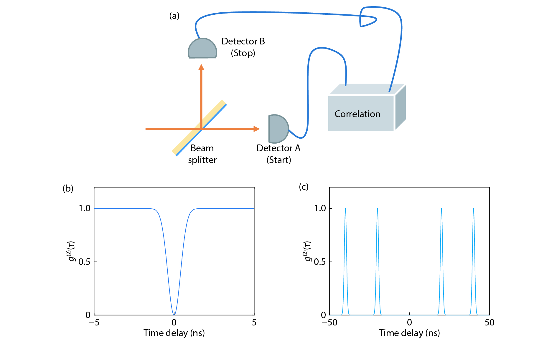
    Fig. 1. (Color online) (a) Schematic diagram of a Hanbury Brown and Twiss experiment. Second-order correlation function (τ) of an ideal SPS working in continuous wave mode (b) and pulse mode (c).
    (Color online) When two indistinguishable photons encounter a beam splitter simultaneously, the two paths in (a) and (b) are observable, while the two paths in (c) interfere destructively and cancel each other.
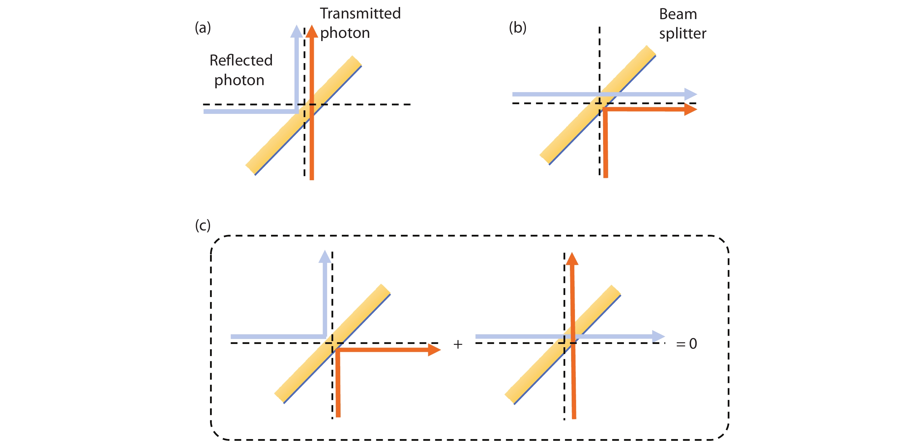
    Fig. 2. (Color online) When two indistinguishable photons encounter a beam splitter simultaneously, the two paths in (a) and (b) are observable, while the two paths in (c) interfere destructively and cancel each other.
    (Color online) (a) Schematic diagram of forming an exciton state in a QD. (b) Spectrum of a single QD. The exciton (X), biexciton (XX ) and singly charged exciton (X+) emission lines were identified at 10 K[30]. Panel (b) adapted with permission from Ref. [30]. Copyright 2013, American Institute of Physics.
    Fig. 3. (Color online) (a) Schematic diagram of forming an exciton state in a QD. (b) Spectrum of a single QD. The exciton (X), biexciton (XX ) and singly charged exciton (X+) emission lines were identified at 10 K[30]. Panel (b) adapted with permission from Ref. [30]. Copyright 2013, American Institute of Physics.
    (Color online) (a) Schematic of a single-photon emitting diode in cross section[12]. (b) Improved device structure by integrating with a planar cavity. The lateral dimensions of the mesa are 60 × 40 m2[13]. (c) Illustration of the indistinguishable-photon emitting diode based on a QD micropillar cavity structure[17]. (d) Structure of an electrically driven SPS based on InP QDs[32]. (e) Schematic of an InGaN dot-in-GaN nanowire p–n junction grown on (111) silicon by MBE. A 2-nm quantum dot is placed at the center of doped GaN regions[14]. (f) Schematic of the heterostructure grown on GaN-on-sapphire by MBE to form a single-photon diode[15]. Panel (a) adapted with permission from Ref. [12]. Copyright 2002, American Association for the Advancement of Science. Panel (b) adapted with permission from Ref. [13]. Copyright 2007, American Institute of Physics. Panel (c) adapted with permission from Ref. [17]. Copyright 2010, American Institute of Physics. Panel (d) adapted with permission from Ref. [31]. Copyright 2008, The Optical Society. Panel (e) adapted with permission from Ref. [14]. Copyright 2013, Springer Nature Publishing AG. Panel (f) adapted with permission from Ref. [15]. Copyright 2014, American Institute of Physics.
    Fig. 4. (Color online) (a) Schematic of a single-photon emitting diode in cross section[12]. (b) Improved device structure by integrating with a planar cavity. The lateral dimensions of the mesa are 60 × 40 m2[13]. (c) Illustration of the indistinguishable-photon emitting diode based on a QD micropillar cavity structure[17]. (d) Structure of an electrically driven SPS based on InP QDs[32]. (e) Schematic of an InGaN dot-in-GaN nanowire p–n junction grown on (111) silicon by MBE. A 2-nm quantum dot is placed at the center of doped GaN regions[14]. (f) Schematic of the heterostructure grown on GaN-on-sapphire by MBE to form a single-photon diode[15]. Panel (a) adapted with permission from Ref. [12]. Copyright 2002, American Association for the Advancement of Science. Panel (b) adapted with permission from Ref. [13]. Copyright 2007, American Institute of Physics. Panel (c) adapted with permission from Ref. [17]. Copyright 2010, American Institute of Physics. Panel (d) adapted with permission from Ref. [31]. Copyright 2008, The Optical Society. Panel (e) adapted with permission from Ref. [14]. Copyright 2013, Springer Nature Publishing AG. Panel (f) adapted with permission from Ref. [15]. Copyright 2014, American Institute of Physics.
    (Color online) (a) Schematic diagram of the key components of a electrically driven SPS based on CQD. (b) curve of a quantum-dot driven at 2.6 V indicates the generation of single-photons with high purity[18]. Panel (a) and (b) adapted with permission from Ref. [18]. Copyright 2017, Springer Nature Publishing AG.
    Fig. 5. (Color online) (a) Schematic diagram of the key components of a electrically driven SPS based on CQD. (b) curve of a quantum-dot driven at 2.6 V indicates the generation of single-photons with high purity[18]. Panel (a) and (b) adapted with permission from Ref. [18]. Copyright 2017, Springer Nature Publishing AG.
    (Color online) (a) Schematic view of a waveguide with integrated single carbon nanotube and two SNSPDs. (b) Optical micrograph of the metallic contacts and the waveguide. The positions of the detectors and emitter are denoted by D and E, respectively[19]. Panel (a) and (b) adapted with permission from Ref. [19]. Copyright 2016, Springer Nature Publishing AG.
    Fig. 6. (Color online) (a) Schematic view of a waveguide with integrated single carbon nanotube and two SNSPDs. (b) Optical micrograph of the metallic contacts and the waveguide. The positions of the detectors and emitter are denoted by D and E, respectively[19]. Panel (a) and (b) adapted with permission from Ref. [19]. Copyright 2016, Springer Nature Publishing AG.
    (Color online) (a) Schematic diagram of STM-induced fluorescence from a single molecule. Molecular fluorescence was generated by the excitation of highly localized tunneling electrons over a single ZnPc molecule that was decoupled by NaCl layers from the Ag(100) substrate. (b) Second-order correlation measurements of single-molecule electroluminescence[20]. Panel (a) and (b) adapted with permission from Ref. [20]. Copyright 2017, Springer Nature Publishing AG.
    Fig. 7. (Color online) (a) Schematic diagram of STM-induced fluorescence from a single molecule. Molecular fluorescence was generated by the excitation of highly localized tunneling electrons over a single ZnPc molecule that was decoupled by NaCl layers from the Ag(100) substrate. (b) Second-order correlation measurements of single-molecule electroluminescence[20]. Panel (a) and (b) adapted with permission from Ref. [20]. Copyright 2017, Springer Nature Publishing AG.
    (Color online) (a) Schematic diagram of the single-photon emitting diode based on NV centers in diamond[22]. (b) Schematic diagrams of SiC SPS and optical measurement setup[24]. Panel (a) adapted with permission from Ref. [22]. Copyright 2012, Macmillan Publishers Limited. Panel (b) adapted with permission from Ref. [24]. Copyright 2015, Springer Nature Publishing AG.
    Fig. 8. (Color online) (a) Schematic diagram of the single-photon emitting diode based on NV centers in diamond[22]. (b) Schematic diagrams of SiC SPS and optical measurement setup[24]. Panel (a) adapted with permission from Ref. [22]. Copyright 2012, Macmillan Publishers Limited. Panel (b) adapted with permission from Ref. [24]. Copyright 2015, Springer Nature Publishing AG.
    (Color online) (a) Optical microscope image of a LED device by vertical stacking of thin layer semiconductors. (b) Confocal microscope image of the electroluminescence from monolayer and bilayer WSe2 areas with an injection current of 3 μA (12.4 V). The dotted circles highlight the submicron localized emission in this device. (c) Second-order correlation measurement of electroluminescence from a single quantum emitter with [50]. Panel (a), (b) and (c) adapted with permission from Ref. [50]. Copyright 2016, Springer Nature Publishing AG.
    Fig. 9. (Color online) (a) Optical microscope image of a LED device by vertical stacking of thin layer semiconductors. (b) Confocal microscope image of the electroluminescence from monolayer and bilayer WSe2 areas with an injection current of 3 μA (12.4 V). The dotted circles highlight the submicron localized emission in this device. (c) Second-order correlation measurement of electroluminescence from a single quantum emitter with [50]. Panel (a), (b) and (c) adapted with permission from Ref. [50]. Copyright 2016, Springer Nature Publishing AG.
    Yating Lin, Yongzheng Ye, Wei Fang. Electrically driven single-photon sources[J]. Journal of Semiconductors, 2019, 40(7): 071904
    Download Citation