
Yating Lin, Yongzheng Ye, Wei Fang. Electrically driven single-photon sources[J]. Journal of Semiconductors, 2019, 40(7): 071904
- Journal of Semiconductors
- Vol. 40, Issue 7, 071904 (2019)
Abstract
1. Introduction
Quantum information techniques are recognized to have greatly enhanced performance in communication, computation, and measurement over the classical ones[
Electrically driven SPS based on semiconductor p–n structure is a straightforward solution to this problem. Once a voltage is applied on such device, carriers can be injected into a single quantum emitter buried in the junction region and single-photons can be generated. Thus, the lack of optical pumping renders the monolithic integration of SPSs and detectors without optical filtering possible. However, additional sophisticated growth and fabrication processes are usually needed to ensure efficient electrical excitation comparing to the optical excitation schemes. Nevertheless, electrically driven SPSs have been realized in various semiconductor systems based on quantum dots (QDs)[
We organize this review as follows: In the second part, we introduce the important properties of a SPS for practical applications, and the ways to characterize them. In the third part, we review recent progresses in electrically driven SPSs based on different solid-state quantum emitters, including quantum confined materials such as semiconductor QDs and carbon nanotubes, single molecules and defect states. Finally, remaining challenges for electrically driven SPSs are discussed.
2. The basics of single-photon sources
An ideal SPS emits exactly one photon at a given time into a particular polarization and spatial mode. From a practical point of view, the most important factors that evaluate the performance of a SPS are single-photon purity, determinacy and brightness. While in many quantum information applications, indistinguishability is also required so that single-photons are identical to each other in all their freedom of degrees.
Single-photon purity denotes how well the source satisfies the SPS criterion that each light pulse generated contains no more than one photon. This property can be characterized by the second-order intensity correlation function
While in quantum mechanics, it can be expressed as:
where
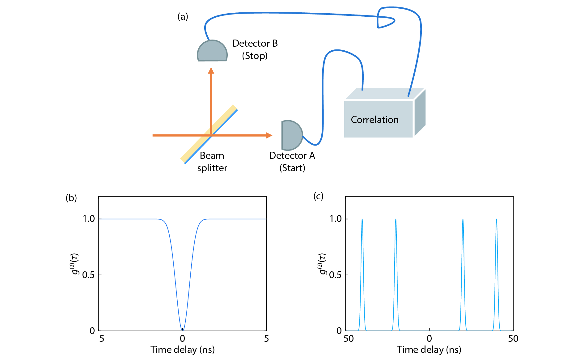
![]()
Figure 1.(Color online) (a) Schematic diagram of a Hanbury Brown and Twiss experiment. Second-order correlation function
As mentioned above, SPSs can not be prepared from a classical light source, as either a coherent or a thermal light source will always generate multi-photons at the same time with certain probability, no matter how such a source is attenuated. There are mainly two ways to generate single-photons. The most widely used SPSs are based on spontaneous parametric down-conversion or spontaneous four-wave mixing. However the nonlinear optical processes occur randomly, and single-photons are generated in a probabilistic way. On the other hand, quantum emitter based on a single two-level system can generate single-photons in a deterministic way (on-demand) under certain excitation condition[
However, in the real world, there always exists loss in the system. Even an deterministic source will be probabilistic when the optical loss increases. The property of brightness implies the overall probability of collecting photons when the loss of a the system is considered. Together with the source repetition rate, brightness determines the speed of quantum information process, which is critical for system scaling.
Indistinguishable single-photons are essential for many quantum applications, especially in constructing quantum gates. The property that photons hardly interact with each other hinders the implement of nonlinear optics schemes in scalable quantum information processes. The linear optical protocol which uses linear optical elements, single-photons and photon detectors can solve this problem, however requiring the single-photons to be indistinguishable. Indistinguishability can be characterized by Hong-Ou-Mandel (HOM) interference[
![]()
Figure 2.(Color online) When two indistinguishable photons encounter a beam splitter simultaneously, the two paths in (a) and (b) are observable, while the two paths in (c) interfere destructively and cancel each other.
The degree of indistinguishability can be evaluated by HOM visibility. In practice, the HOM visibility may not reach unity due to the coupling between the quantum emitter and environment, especially for a solid-state system. Phonon interaction and fluctuating electric/magnetic field will introduce dephasing that shorten the coherence time of the photon, and thus lower the degree of indistinguishability of generated single-photons.
Other than the factors discussed above, for practical applications, there also exist other essential standards for SPSs like working at room temperature, pump by electricity, emission spectral range and so on.
3. Electrically driven single-photon sources
SPSs based on the optical pump are more mature than those driven by electricity. However, the demands of fully integrated quantum photonic circuits promote the development of electrically driven SPSs. Of the two schemes that may generate single-photons, the nonlinear optical processes can not be realized by electrical pumping. For a two-level like system, the spontaneous relaxation from excited state to the ground state will emit one, and only one, photon at a time. SPSs based on single quantum emitters have been demonstrated in systems such as atoms, ions, molecules, defect states and semiconductor QDs. Fortunately, most of the solid-state emitters are compatible with electrical excitation scheme. To efficient inject carriers into a electrically driven SPS and populate the excited state, the device usually incorporates a p–n junction to form a single-photon emitting diode. In the following part, we explore realizations of electrically driven SPSs based on various solid-state systems in detail.
3.1. Semiconductor quantum dots
An early proposal on electrically driven SPS was utilizing the Coulomb blockade and quantum confinement effects based on a mesoscopic semiconductor p–i–n heterostructure[
![]()
Figure 3.(Color online) (a) Schematic diagram of forming an exciton state in a QD. (b) Spectrum of a single QD. The exciton (X), biexciton (XX ) and singly charged exciton (X+) emission lines were identified at 10 K[
There are a couple of types of QDs that can be used as solid-state SPSs. Epitaxial QDs grown by molecular beam epitaxy (MBE) or metal-organic chemical vapour deposition (MOCVD) in the Stranski-Krastanov mode are the most widely studied ones. A lattice-mismatched material is firstly grown on a semiconductor substrate to form an epitaxial wetting layer. When the thickness of this layer reaches a critical value, tiny self-assembled islands start to form in order to minimize the surface strain. Various material systems have been investigated as candidates for epitaxial QDs, such as III–V arsenide, phosphide or nitride based QDs, II–VI telluride or selenide based QDs, with emission wavelengths ranging from ultraviolet to telecom wavelength. Though many of the epitaxial QDs work at cryogenic temperature, QDs based on wide band gap semiconductors may operate at high or room temperature.
At present, the best-performing QD-based SPSs are made of InAs/GaAs QDs. Fig. 3(b) shows a typical low temperature photoluminescence spectrum of a single QD. Here multiple excitation states can be observed, which may degrade the single-photon properties. Fortunately due to Coulomb interaction, photons from exciton state (X), biexciton state (XX) and charged exciton (X+, exciton with an extra hole) have distinct energies. Thus a spectral filtering mechanism is usually needed to single out just one emission line, either externally or via microcavity resonance. SPSs with high single-photon purity and indistinguishability have been reported based on InAs QDs, though via optical excitation[
The epitaxial growth procedure of QDs makes them feasible to be integrated in conventional p–i–n light emitting diode (LED) structure. In 2002, shields et al. presented the first electrically driven SPS, as shown in Fig. 4(a). The semiconductor layer was grown by MBE and the InAs QDs were inserted into the intrinsic region. Working at 5 K, the single QD emission exhibited two sharp emission lines, which respectively represented exciton and biexciton peaks. By extracting the exciton electroluminescence, the clear anti-bunching of the second-order correlation function under continuous or pulse drive indicated single-photon generation. Due to the high refractive index of GaAs material, the single-photon extracting efficiency was very low. This structure was subsequently improved by integrating a planar cavity with the LED, as shown in Fig. 4(b)[
![]()
Figure 4.(Color online) (a) Schematic of a single-photon emitting diode in cross section[
Though the performance of InAs QD based SPSs at low temperature are promising via either optical or electrical excitation, their applications at higher or room temperature are difficult due to the low exciton bondage energy. III–V epitaxial phosphide or nitride based QDs that possess larger exciton bondage energies have been explored with blue shifted working wavelength range. Electrically driven SPS based on InP QDs working at 80 K was demonstrated, and the emission was in the red spectral range (670 nm)[
Semiconductor colloidal QDs (CQDs), or nanocrystals, synthesized by wet chemical approaches are another kind of QDs that have been studied extensively as room-temperature sources of single-photons since the first report in 2000[
![]()
Figure 5.(Color online) (a) Schematic diagram of the key components of a electrically driven SPS based on CQD. (b)
3.2. Carbon nanotubes
Other than the three-dimensionally confined (or zero-dimensional material) QDs, two-dimensionally confined (or one-dimensional material) semiconductors such as single-walled carbon nanotubes have been reported as single-photon emitters at low temperature[
The first full integrated quantum photonic circuit was demonstrated in carbon nanotube system[
![]()
Figure 6.(Color online) (a) Schematic view of a waveguide with integrated single carbon nanotube and two SNSPDs. (b) Optical micrograph of the metallic contacts and the waveguide. The positions of the detectors and emitter are denoted by D and E, respectively[
3.3. Single molecules
Unlike quantum confined semiconductor systems whose emission energies can be tuned by the sizes of nanostructures, molecules are atomic like systems with fixed electronic states. Different from atom systems, vibrations and phonons are usually strongly involved in luminescence of molecular systems. The excitation of phonon states are strongly dependent on temperature. At low temperature, only the lowest lattice vibration is excited. So the transition between the ground electronic state and excited electronic state shows a very narrow line which is called the zero-phonon line[
Organic fluorescent molecules have for a long time served as a tool for imaging and lighting. And the optically excited dye molecule SPS demonstrated in 2000 is the poineering work for room-temperature SPSs based on quantum emitters[
Interestingly, the first demonstration of electrically driven molecule SPS was based on a technique called scanning tunneling microscope (STM) induced luminescence[
![]()
Figure 7.(Color online) (a) Schematic diagram of STM-induced fluorescence from a single molecule. Molecular fluorescence was generated by the excitation of highly localized tunneling electrons over a single ZnPc molecule that was decoupled by NaCl layers from the Ag(100) substrate. (b) Second-order correlation measurements of single-molecule electroluminescence[
3.4. Defect states
A defect state in a crystal, either a missing atom or an impurity atom, introduces a narrow level within bandgap of the crystal material. If transition between such defect level and the ground level absorbs or emits a photon in visible spectrum, the crystal that is usually transparent becomes colored. So defect states are sometimes called color centers in wide bandgap semiconductors. Similar as single molecule, radiative relaxation from a defect state to the ground electronic state will generate sharp ZPL, while broad phonon sideband may show up at room temperature.
Color centers in diamond, particularly nitrogen-vacancy (NV) centers, are prominent candidates for SPSs due to their excellent photostability at room temperature[
The difficulties of realizing electrically driven SPSs based on color centers lie on the synthesis of the electron (n-type) and hole (p-type) conducting materials as well as an ultra-pure intrinsic (i) layers to build up p–i–n diode structures. The first approach was reported in 2011, where the in-plane diodes were fabricated on a high quality single crystal diamond grown by chemical vapor deposition, with implantation of boron and phosphorus ions to form doping p-type and n-type areas, respectively[
![]()
Figure 8.(Color online) (a) Schematic diagram of the single-photon emitting diode based on NV centers in diamond[
Similar to color centers in diamond, single defects in other wide-bandgap semiconductors such as silicon carbide (SiC) and zinc oxide (ZnO) are also possible solutions for room-temperature electrically driven SPSs. ZnO has attractive emission range in ultraviolet and visible spectral with the high exciton binding energy (60 meV)[
Thin layers of semiconducting transition-metal dichalcogenides (TMDs) are emerging platforms for both scientific study and technological applications, providing the potential to be integrated into conventional optoelectronic systems[
![]()
Figure 9.(Color online) (a) Optical microscope image of a LED device by vertical stacking of thin layer semiconductors. (b) Confocal microscope image of the electroluminescence from monolayer and bilayer WSe2 areas with an injection current of 3
4. Summary and outlook
In summary, we have overviewed recent progresses in electrically driven solid-state SPSs for integrated quantum photonics. For all of the realizations, epitaxial InAs QDs exhibit the best performance in terms of single-photon purity and indistinguishability, however, cryogenic environments are usually needed. Wide bandgap epitaxial QDs, colloidal QDs, molecules and many defect states based SPSs show the ability to operate at room temperature, which are favorable for practical applications. Quantum emitters in their freestanding form have the flexibility to integrate with other structures and devices on various substrates, as single carbon nanotubes have demonstrated the monolithic integration of SPS with single-photon detectors.
Despite many remarkable progresses have been done so far, the complex mesoscopic environment of the p-n junction structure entails numerous challenges. Suppressing background emission from auxiliary structures and other excited states is the key to generate single-photons with high purity from integrated SPSs. Fluctuating charges around a quantum emitter can create a fluctuating electric field that gives rise to photon distinguishability from the same emitter under electrical excitation, though such effect can be suppressed to a certain extent by incorporating a microcavity. Moreover, unlike the optical
Acknowledgments
We acknowledge the financial support from the National Key R&D Program of China (No. 2016YFB0401600), the National Natural Science Foundation of China (No. 61635009), and the Fundamental Research Funds for the Central Universities (No. 2018FZA5004).
References
[1]
[2] Q C Sun, Y L Mao, S J Chen et al. Quantum teleportation with independent sources and prior entanglement distribution over a network. Nat Photon, 10, 671(2016).
[3] J L O’brien. Optical quantum computing. Science, 318, 1567(2007).
[4] M Arcari, I Söllner, A Javadi et al. Near-unity coupling efficiency of a quantum emitter to a photonic crystal waveguide. Phys Rev Lett, 113, 093603(2014).
[5] J Carolan, C Harrold, C Sparrow et al. Universal linear optics. Science, 349, 711(2015).
[6] J Wang, S Paesani, Y Ding et al. Multidimensional quantum entanglement with large-scale integrated optics. Science, 360, 285(2018).
[7] B J Smith, D Kundys, N Thomas-Peter et al. Phase-controlled integrated photonic quantum circuits. Opt Express, 17, 13516(2009).
[8] H Takesue, N Matsuda, E Kuramochi et al. An on-chip coupled resonator optical waveguide single-photon buffer. Nat Commun, 4, 2725(2013).
[9] W H Pernice, C Schuck, O Minaeva et al. High-speed and high-efficiency travelling wave single-photon detectors embedded in nanophotonic circuits. Nat Commun, 3, 1325(2012).
[10] J Sprengers, A Gaggero, D Sahin et al. Waveguide superconducting single-photon detectors for integrated quantum photonic circuits. Appl Phys Lett, 99, 181110(2011).
[11] P Senellart, G Solomon, A White. High-performance semiconductor quantum-dot single-photon sources. Nat Nano, 12, 1026(2017).
[12] Z Yuan, B E Kardynal, R M Stevenson et al. Electrically driven single-photon source. Science, 295, 102(2002).
[13] M Ward, T Farrow, P See et al. Electrically driven telecommunication wavelength single-photon source. Appl Phys Lett, 90, 063512(2007).
[14] S Deshpande, J Heo, A Das et al. Electrically driven polarized single-photon emission from an InGaN quantum dot in a GaN nanowire. Nat Commun, 4, 1675(2013).
[15] S Deshpande, T Frost, A Hazari et al. Electrically pumped single-photon emission at room temperature from a single In- GaN/GaN quantum dot. Appl Phys Lett, 105, 141109(2014).
[16] A Nowak, S Portalupi, V Giesz et al. Deterministic and electrically tunable bright single-photon source. Nat Commun, 5, 3240(2014).
[17] T Heindel, C Schneider, M Lermer et al. Electrically driven quantum dot-micropillar single photon source with 34% overall efficiency. Appl Phys Lett, 96, 011107(2010).
[18] X Lin, X Dai, C Pu et al. Electrically-driven single-photon sources based on colloidal quantum dots with near-optimal antibunching at room temperature. Nat Commun, 8, 1132(2017).
[19] S Khasminskaya, F Pyatkov, K Słowik et al. Fully integrated quantum photonic circuit with an electrically driven light source. Nat Photon, 10, 727(2016).
[20] L Zhang, Y J Yu, L G Chen et al. Electrically driven single-photon emission from an isolated single molecule. Nat Commun, 8, 580(2017).
[21] A Lohrmann, S Pezzagna, I Dobrinets et al. Diamond based light-emitting diode for visible single-photon emission at room temperature. Appl Phys Lett, 99, 251106(2011).
[22] N Mizuochi, T Makino, H Kato et al. Electrically driven single-photon source at room temperature in diamond. Nat Photon, 6, 299(2012).
[23] Y Doi, T Makino, H Kato et al. Deterministic electrical charge-state initialization of single nitrogen-vacancy center in diamond. Phys Rev X, 4, 011057(2014).
[24] A Lohrmann, N Iwamoto, Z Bodrog et al. Single-photon emitting diode in silicon carbide. Nat Commun, 6, 7783(2015).
[25] R J Glauber. The quantum theory of optical coherence. Phys Rev, 130, 2529(1963).
[26] R H Brown, R Q Twiss, g surName. Interferometry of the intensity fluctuations in light-i. basic theory: the correlation between photons in coherent beams of radiation. Proceedings of the Royal Society of London Series A Mathematical and Physical Sciences, 242, 300(1957).
[27] H Wang, Z C Duan, Y H Li et al. Near-transform-limited single photons from an efficient solid-state quantum emitter. Phys Rev Lett, 116, 213601(2016).
[28] C K Hong, Z Y Ou, L Mandel. Measurement of subpicosecond time intervals between two photons by interference. Phys Rev Lett, 59, 2044(1987).
[29] A Imamog, Y Yamamoto et al. Turnstile device for heralded single photons: Coulomb blockade of electron and hole tunnel- ing in quantum confined p–i–n heterojunctions. Phys Rev Lett, 72, 210(1994).
[30] M Gschrey, F Gericke, A Schüßler et al. In situ electron-beam lithography of deterministic single-quantum-dot mesa-structures using low-temperature cathodoluminescence spectroscopy. Appl Phys Lett, 102, 251113(2013).
[31] N Somaschi, V Giesz, L De Santis et al. Near-optimal single-photon sources in the solid state. Nat Photonics, 10, 340(2016).
[32] M Reischle, G Beirne, W M Schulz et al. Electrically pumped single-photon emission in the visible spectral range up to 80 K. Opt Express, 16, 12771(2008).
[33] A Schlehahn, A Thoma, P Munnelly et al. An electrically driven cavity-enhanced source of indistinguishable photons with 61% overall efficiency. APL Photon, 1, 011301(2016).
[34] S Deshpande, P Bhattacharya. An electrically driven quantum dot-in-nanowire visible single photon source operating up to 150 K. Appl Phys Lett, 103, 241117(2013).
[35] W Quitsch, T Kümmell, A Gust et al. Electrically driven single photon emission from a CdSe/ZnSSe single quantum dot at 200 K. Appl Phys Lett, 105, 091102(2014).
[36] P Michler, A Imamoglu, M Mason et al. Quantum correlation among photons from a single quantum dot at room temperature. Nature, 406, 968(2000).
[37] A Högele, C Galland, M Winger et al. Photon antibunching in the photoluminescence spectra of a single carbon nanotube. Phys Rev Lett, 100, 217401(2008).
[38]
[39] B Lounis, W E Moerner. Single photons on demand from a single molecule at room temperature. Nature, 407, 491(2000).
[40] M Nothaft, S Höhla, F Jelezko et al. Electrically driven photon antibunching from a single molecule at room temperature. Nat Commun, 3, 628(2012).
[41] M W Doherty, N B Manson, P Delaney et al. The nitrogen-vacancy colour centre in diamond. Phys Rep, 528, 1(2013).
[42] I A Khramtsov, M Agio, D Y Fedyanin. Dynamics of single-photon emission from electrically pumped color centers. Phys Rev Appl, 8, 024031(2017).
[43] Ü Özgür, Y I Alivov, C Liu et al. A comprehensive review of ZnO materials and devices. J Appl Phys, 98, 041301(2005).
[44] S Choi, A M Berhane, A Gentle et al. Electroluminescence from localized defects in zinc oxide: toward electrically driven single photon sources at room temperature. ACS Appl Mater Interfaces, 7, 5619(2015).
[45] I A Khramtsov, A A Vyshnevyy, D Y Fedyanin. Enhancing the brightness of electrically driven single-photon sources using color centers in silicon carbide. npj Quantum Inform, 4, 15(2018).
[46] S Manzeli, D Ovchinnikov, D Pasquier et al. 2D transition metal dichalcogenides. Nat Rev Mater, 2, 17033(2017).
[47] M Koperski, K Nogajewski, A Arora et al. Single photon emitters in exfoliated WSe2 structures. Nat Nano, 10, 503(2015).
[48] C Chakraborty, L Kinnischtzke, K M Goodfellow et al. Voltage-controlled quantum light from an atomically thin semicon- ductor. Nat Nano, 10, 507(2015).
[49] Y M He, G Clark, J R Schaibley et al. Single quantum emitters in monolayer semiconductors. Nat Nano, 10, 497(2015).
[50] C Palacios-berraquero, M Barbone, D M Kara et al. Atomically thin quantum light-emitting diodes. Nat Commun, 7, 12978(2016).
[51] T T Tran, K Bray, M J Ford et al. Quantum emission from hexagonal boron nitride monolayers. Nat Nano, 11, 37(2016).
[52] M Conterio, N Sköld, D Ellis et al. A quantum dot single photon source driven by resonant electrical injection. Appl Phys Lett, 103, 162108(2013).

Set citation alerts for the article
Please enter your email address
© Copyright 2018-2021 | Chinese Laser Press. All Rights Reserved 沪ICP备15018463号-20