• Laser & Optoelectronics Progress
  • Vol. 58, Issue 21, 2106004 (2021)
Zhiqiang Chen1、2、**, Linghao Cheng1, Yuan Bao2、*, Dawei Liu2, Jianlin Fan2, and Zhitao Chen2
Author Affiliations
  • 1Institute of Photonics Technology, Jinan University, Guangzhou , Guangdong 510632, China
  • 2Institute of Semiconductors, Guangdong Academy of Sciences, Guangzhou , Guangdong 510651, China
  • show less
    DOI: 10.3788/LOP202158.2106004 Cite this Article Set citation alerts
    Zhiqiang Chen, Linghao Cheng, Yuan Bao, Dawei Liu, Jianlin Fan, Zhitao Chen. Architecture of Reconfigurable Transmitter Integrated Circuits for Four-Level Pulse Amplitude Modulation Optical Interconnection System[J]. Laser & Optoelectronics Progress, 2021, 58(21): 2106004 Copy Citation Text show less
    Block diagram of the PAM4 optical interconnection system
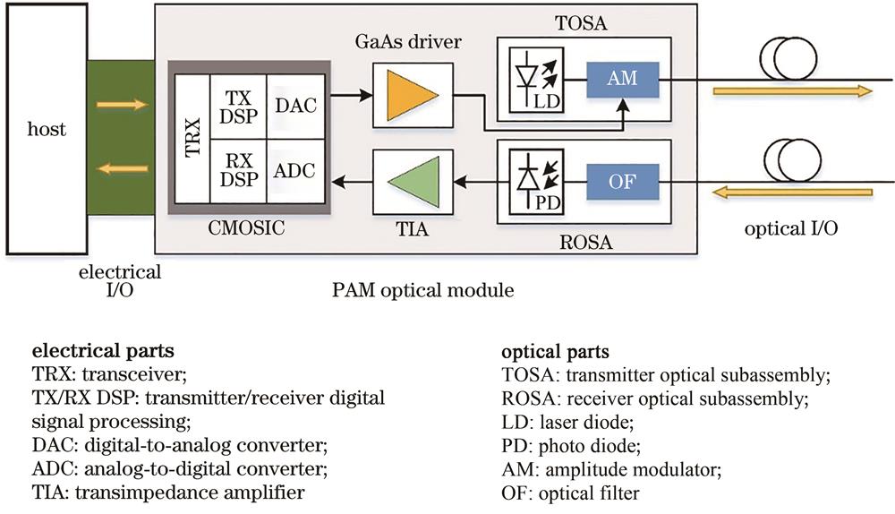
    Fig. 1. Block diagram of the PAM4 optical interconnection system
    Architecture of 40 Gbit/s PAM4 transmitter IC
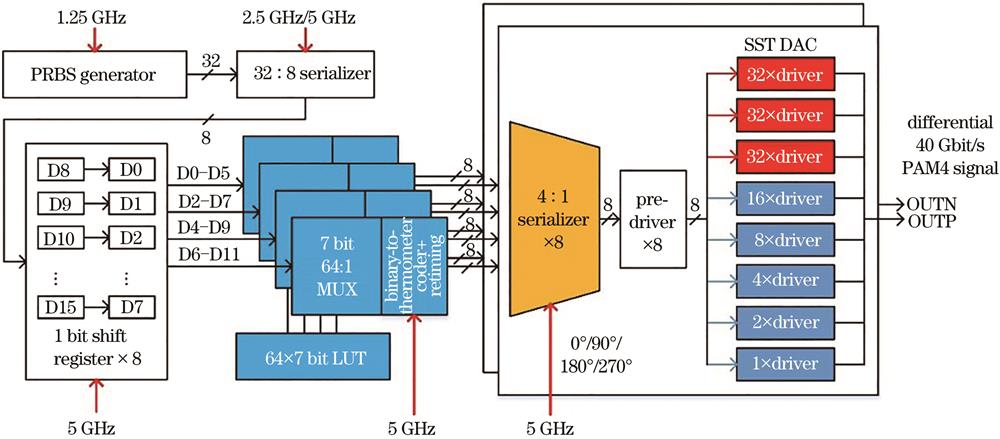
    Fig. 2. Architecture of 40 Gbit/s PAM4 transmitter IC
    Architecture of pipelined 64∶1 MUX. (a) Overview circuit; (b) 3 stage pipeline structure; (c) 4∶1 MUX ;(d) dynamic latch and dynamic DFF
    Fig. 3. Architecture of pipelined 64∶1 MUX. (a) Overview circuit; (b) 3 stage pipeline structure; (c) 4∶1 MUX ;(d) dynamic latch and dynamic DFF
    4∶1 serializer and pre-driver. (a) Circuit structure; (b) synthesis principle of the serializer signal; (c) circuit of 1 UI pulse generator; (d) structure of the pseudo AND gate
    Fig. 4. 4∶1 serializer and pre-driver. (a) Circuit structure; (b) synthesis principle of the serializer signal; (c) circuit of 1 UI pulse generator; (d) structure of the pseudo AND gate
    Structure of the DAC
    Fig. 5. Structure of the DAC
    Layout and simulation. (a) Layout of circuits block; (b) output eye diagram with no equalization; (c) relationship between eye diagram jitter and feedback resistor
    Fig. 6. Layout and simulation. (a) Layout of circuits block; (b) output eye diagram with no equalization; (c) relationship between eye diagram jitter and feedback resistor
    Output eye diagrams with different LUT equalization mode. (a) 2-tap FFE; (b) 3-tap FFE; (c) nonlinear equalization without FFE; (d) nonlinear equalization with 3-tap FFE
    Fig. 7. Output eye diagrams with different LUT equalization mode. (a) 2-tap FFE; (b) 3-tap FFE; (c) nonlinear equalization without FFE; (d) nonlinear equalization with 3-tap FFE
    Circuit blockDelay t
    Clock duty Tc200
    2-4 coder68

    Driver fanout(pipeline 1)

    64∶16 MUX(pipeline 1)

    16∶4 MUX(pipeline 2)

    4∶1 MUX(pipeline 3)

    Dynamic DFF and latch’s Tsetup

    Dynamic DFF and latch’s Tclk-Q

    Dynamic latch’s TD-Q

    77

    81

    78

    67

    25

    43

    37

    Table 1. Post simulation results of the delay of each level of pipeline module in 64∶1 MUX
    Zhiqiang Chen, Linghao Cheng, Yuan Bao, Dawei Liu, Jianlin Fan, Zhitao Chen. Architecture of Reconfigurable Transmitter Integrated Circuits for Four-Level Pulse Amplitude Modulation Optical Interconnection System[J]. Laser & Optoelectronics Progress, 2021, 58(21): 2106004
    Download Citation