• Opto-Electronic Advances
  • Vol. 3, Issue 10, 200011-1 (2020)
Kiyosh Asakawa1、*, Yoshimasa Sugimoto2, and Shigeru Nakamura3
Author Affiliations
  • 1Associate Program, University of Tsukuba, Tsukuba, Ibaraki 305-8571, Japan
  • 2Nanotechnology Innovation Station, National Institute for Materials Science (NIMS), 1-2-1 Sengen, Tsukuba, Ibaraki 305-0047, Japan
  • 3Biometrics Research Laboratories, NEC Corporation, 1131, Hinode, Abiko, Chiba 270-1198, Japan
  • show less
    DOI: 10.29026/oea.2020.200011 Cite this Article
    Kiyosh Asakawa, Yoshimasa Sugimoto, Shigeru Nakamura. Silicon photonics for telecom and data-com applications[J]. Opto-Electronic Advances, 2020, 3(10): 200011-1 Copy Citation Text show less
    History of the traffic among human beings1.
    Fig. 1. History of the traffic among human beings1.
    Progresses in the optical communication network2.
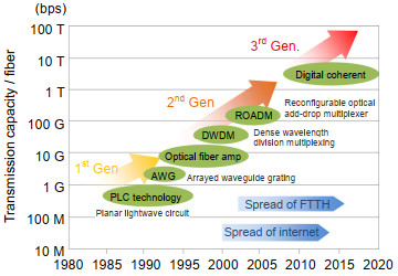
    Fig. 2. Progresses in the optical communication network2.
    Demonstration of the first optical grating connected to silicon waveguides by Luxtera. Figure reproduced from ref.6, under a Creative Commons Attribution License.
    Fig. 3. Demonstration of the first optical grating connected to silicon waveguides by Luxtera. Figure reproduced from ref.6, under a Creative Commons Attribution License.
    (a–c) SEM images of a single-mode strip waveguide cross-section at different orientations. (d, e) Bending loss spectra for TE and TM polarizations, respectively. Figure reprinted with permission from ref.14, Optical Society of America.
    Fig. 4. (a–c) SEM images of a single-mode strip waveguide cross-section at different orientations. (d, e) Bending loss spectra for TE and TM polarizations, respectively. Figure reprinted with permission from ref.14, Optical Society of America.
    Schematic of VCSEL with Si HCG as bottom mirror.(a) Tilted-view of VCSEL cross-section with circulating red arrows indicating optical cavity. (b) The VCSEL employs a proton implant-defined aperture for current confinement, indicated by red curved lines between contacts. Figure reprinted with permission from ref.27, Optical Society of America.
    Fig. 5. Schematic of VCSEL with Si HCG as bottom mirror. (a) Tilted-view of VCSEL cross-section with circulating red arrows indicating optical cavity. (b) The VCSEL employs a proton implant-defined aperture for current confinement, indicated by red curved lines between contacts. Figure reprinted with permission from ref.27, Optical Society of America.
    Schematic layer structure of an InAs/GaAs QD laser on a Ge-on-Si substrate. Figure reprinted with permission from ref.31, Optical Society of America.
    Fig. 6. Schematic layer structure of an InAs/GaAs QD laser on a Ge-on-Si substrate. Figure reprinted with permission from ref.31, Optical Society of America.
    SEM photographs of nano-scale Si/SiO2 waveguides.(a, b) Multiply coupled micro-rings and their magnified ones. (c) Sharp taper. Figure reprinted with permission from ref.10, SPIE.
    Fig. 7. SEM photographs of nano-scale Si/SiO2 waveguides. (a, b) Multiply coupled micro-rings and their magnified ones. (c) Sharp taper. Figure reprinted with permission from ref.10, SPIE.
    (a) Schematic showing the operating principle of the AWG. (b) Photomicrograph of the AWG with about 1.4 mm square and eight wavelength channels. (c) Filter spectral characteristics. Figure reprinted with permission from: (b, c) ref.38, OKI Corporate.
    Fig. 8. (a) Schematic showing the operating principle of the AWG. (b) Photomicrograph of the AWG with about 1.4 mm square and eight wavelength channels. (c) Filter spectral characteristics. Figure reprinted with permission from: (b, c) ref.38, OKI Corporate.
    Basic block diagram of an optical link including a transmitter and receiver.
    Fig. 9. Basic block diagram of an optical link including a transmitter and receiver.
    50 Gb/s Si photonics transmit module.(a) and (b) are transmitter and receiver, respectively, with wavelength division multiplexing. Figure reproduced from ref.43, Intel.
    Fig. 10. 50 Gb/s Si photonics transmit module. (a) and (b) are transmitter and receiver, respectively, with wavelength division multiplexing. Figure reproduced from ref.43, Intel.
    Silicon photonics shipments, for datacenter (in units) 2019-2025e.(Source: Silicon Photonics report, Yole Développement, 2020)
    Fig. 11. Silicon photonics shipments, for datacenter (in units) 2019-2025e. (Source: Silicon Photonics report, Yole Développement, 2020)
    Si photonic MCM.(a) Photonic integrated circuit (PIC) with flip-chip mounted laser die and edge-coupled waveguide. (b) Logic, HMC and PIC mounted directly to a BGA substrate. (c) Logic and HBM mounted on a high-density interposer with micro-bumps. (d) Cut-away revealing copper pillar, flip-chip, BGA and optoelectronic interconnections. Figure reprinted with permission from ref.52, IBM.
    Fig. 12. Si photonic MCM. (a) Photonic integrated circuit (PIC) with flip-chip mounted laser die and edge-coupled waveguide. (b) Logic, HMC and PIC mounted directly to a BGA substrate. (c) Logic and HBM mounted on a high-density interposer with micro-bumps. (d) Cut-away revealing copper pillar, flip-chip, BGA and optoelectronic interconnections. Figure reprinted with permission from ref.52, IBM.
    IBM Si CWDM 4 × 25 Gb/s die.(a) Photograph of CMOS integrated Si photonics chip. (b) Die with an array of 100 μm Pb-free flip-chip bumps on a 200 μm pitch. Two optical I/Os are seen at the bottom of the die. (c) Transmitter and receiver elements along with their eye diagrams Figure reprinted with permission from ref.52, IBM.
    Fig. 13. IBM Si CWDM 4 × 25 Gb/s die. (a) Photograph of CMOS integrated Si photonics chip. (b) Die with an array of 100 μm Pb-free flip-chip bumps on a 200 μm pitch. Two optical I/Os are seen at the bottom of the die. (c) Transmitter and receiver elements along with their eye diagrams Figure reprinted with permission from ref.52, IBM.
    Schematic cross-section of 45 nm SOI CMOS process based Si photonic platform with photonic as well as electronic devices at the front end and bump at the back end. Figure reprinted with permission from ref.56, IEEE.
    Fig. 14. Schematic cross-section of 45 nm SOI CMOS process based Si photonic platform with photonic as well as electronic devices at the front end and bump at the back end. Figure reprinted with permission from ref.56, IEEE.
    Photograph of "Zero-change" SOI platform die.(a) SoC including a RISC-V processor, SRAM based cache memory and DWDM optical I/Os. (b) WDM transceivers. (c) Key photonic devices of an optical link. Figure reprinted with permission from ref.11, Optical Society of America. Development timeline in Fig. 3, ref.11 has been omitted here.
    Fig. 15. Photograph of "Zero-change" SOI platform die. (a) SoC including a RISC-V processor, SRAM based cache memory and DWDM optical I/Os. (b) WDM transceivers. (c) Key photonic devices of an optical link. Figure reprinted with permission from ref.11, Optical Society of America. Development timeline in Fig. 3, ref.11 has been omitted here.
    40 Gb/s transmitters.(a) Micrograph of the 40 Gb/s NRZ transmitter. (b) NRZ transmission eye-diagram. Figure reprinted with permission from ref.11, Optical Society of America. Figs. 7(b) and 7(d) in ref.11 have been omitted here.
    Fig. 16. 40 Gb/s transmitters. (a) Micrograph of the 40 Gb/s NRZ transmitter. (b) NRZ transmission eye-diagram. Figure reprinted with permission from ref.11, Optical Society of America. Figs. 7(b) and 7(d) in ref.11 have been omitted here.
    (a) Whole part of optical I/O core chip. (b, c) Cross-sectional views of receiver and transmitter, respectively. Figure reprinted with permission from ref.61. AIOCORE.
    Fig. 17. (a) Whole part of optical I/O core chip. (b, c) Cross-sectional views of receiver and transmitter, respectively. Figure reprinted with permission from ref.61. AIOCORE.
    Cross-sectional view of Si photonics integrated circuit with FP-LD. Figure reprinted with permission from ref.60, The Institute of Electronics, Information and Communication Engineers.
    Fig. 18. Cross-sectional view of Si photonics integrated circuit with FP-LD. Figure reprinted with permission from ref.60, The Institute of Electronics, Information and Communication Engineers.
    Transmission characteristics of the optical I/O core with two kinds of MMFs. Figure reprinted with permission from ref.60, The Institute of Electronics, Information and Communication Engineers.
    Fig. 19. Transmission characteristics of the optical I/O core with two kinds of MMFs. Figure reprinted with permission from ref.60, The Institute of Electronics, Information and Communication Engineers.
    Schematic of typical optical switch topologies.(a) Crossbar. (b) PILOSS. (c) Beneš. (d) Switch-and-select. Figure reprinted with permission from ref.66, Optical Society of America.
    Fig. 20. Schematic of typical optical switch topologies. (a) Crossbar. (b) PILOSS. (c) Beneš. (d) Switch-and-select. Figure reprinted with permission from ref.66, Optical Society of America.
    (a) Example of multi-ring network. (b) 4-degree ROADM node configuration connecting two ring networks. Figure reprinted with permission from ref.69, NTT Technical Review.
    Fig. 21. (a) Example of multi-ring network. (b) 4-degree ROADM node configuration connecting two ring networks. Figure reprinted with permission from ref.69, NTT Technical Review.
    (a) Two cases of reconfiguring optical paths in photonic networks with CDC-ROADMs. (b) Schematic of CDC-ROADM. (c) TPA consisting of multiple optical switch modules. (d) Configuration of 8 × 8 multi-cast optical switch. Figure reprinted with permission from ref.75, IEEE.
    Fig. 23. (a) Two cases of reconfiguring optical paths in photonic networks with CDC-ROADMs. (b) Schematic of CDC-ROADM. (c) TPA consisting of multiple optical switch modules. (d) Configuration of 8 × 8 multi-cast optical switch. Figure reprinted with permission from ref.75, IEEE.
    32 × 32 Si TO MZI-based PILOSS switch. Figure reprinted with permission from ref.84, Optical Society of America.
    Fig. 26. 32 × 32 Si TO MZI-based PILOSS switch. Figure reprinted with permission from ref.84, Optical Society of America.
    Transmission characteristics of the six sampled optical paths 1-12, 1-20, 1-32, 32-1, 32-13, and 32-19.(a) Path on the PILOSS switch matrix. (b) On-chip loss. Inset in (b) shows the spectral passband of the path 32-1. Figure reprinted with permission from ref.84, Optical Society of America.
    Fig. 27. Transmission characteristics of the six sampled optical paths 1-12, 1-20, 1-32, 32-1, 32-13, and 32-19. (a) Path on the PILOSS switch matrix. (b) On-chip loss. Inset in (b) shows the spectral passband of the path 32-1. Figure reprinted with permission from ref.84, Optical Society of America.
    32 × 32 Si EO MZI-based Beneš switch. Figure reprinted with permission from ref.90, under a Creative Commons Attribution 4.0 International License.
    Fig. 28. 32 × 32 Si EO MZI-based Beneš switch. Figure reprinted with permission from ref.90, under a Creative Commons Attribution 4.0 International License.
    (a) Schematic configuration of hybrid Si free-space source with integrated beam steering. (b) Layout of the overall devices. Figure reprinted with permission from ref.104, SPIE.
    Fig. 29. (a) Schematic configuration of hybrid Si free-space source with integrated beam steering. (b) Layout of the overall devices. Figure reprinted with permission from ref.104, SPIE.
    (a) Measured beam profiles at 1555 nm wavelength as the beam was swept across the field of view in the ψ axis at 1° increments. (b) Plots of the 2D beam profiles at the corners and center of the field of view. Figure reprinted with permission from ref.109, Optical Society of America.
    Fig. 30. (a) Measured beam profiles at 1555 nm wavelength as the beam was swept across the field of view in the ψ axis at 1° increments. (b) Plots of the 2D beam profiles at the corners and center of the field of view. Figure reprinted with permission from ref.109, Optical Society of America.
    (a) Schematic of the solid-state LiDAR system with transmitting and receiving optical phased arrays. (b) 3D picture of the optical phased array. (c–e) SEM images of phase shifter, magnified one and antenna, respectively. (f) Optical micrograph of the device. Figure reprinted with permission from ref.117, Optical Society of America.
    Fig. 31. (a) Schematic of the solid-state LiDAR system with transmitting and receiving optical phased arrays. (b) 3D picture of the optical phased array. (c–e) SEM images of phase shifter, magnified one and antenna, respectively. (f) Optical micrograph of the device. Figure reprinted with permission from ref.117, Optical Society of America.
    Table 1. Silicon photonics supply chain for optical transceivers41. (Source: Silicon Photonics report, Yole Développement, 2020)
    2017rank2016rankCompanyFoundrytypeLocation2015 sales($M)2016 sales($M)2016/2015change (%)2017 sales($M)2017/2016change (%)
    *Includes Huahong Grace and Shanghai Huali.Source: IC Insights company reports
    11TSMCPure-PlayTaiwan, China26, 57429, 4881132, 1639
    22GlobalFoundriesPure-PlayU.S.5, 0195, 49596, 06010
    33UMCPure-PlayTaiwan, China4, 4644, 58234, 8987
    44SamsungIDMSouth Korea2, 6704, 410654, 6004
    55SMICPure-PlayChina2, 2362, 914303, 1016
    66PowerchipPure-PlayTaiwan, China1, 2681, 27511, 49817
    78Huahong Group*Pure-PlayChina9711, 184221, 39518
    87Tower JazzPure-PlayIsrael9611, 250301, 38811
    Top & Total44, 16350, 5981555, 1039
    Top & Share87%88%88%
    Other Foundry6, 5977, 11287, 2071
    Total Foundry50, 76057, 7101462, 3108
    Table 2. Major 2017 foundries (Pure-Play and IDM (integrated device manufacturer)). Table reprinted with permission from ref.42.
    Kiyosh Asakawa, Yoshimasa Sugimoto, Shigeru Nakamura. Silicon photonics for telecom and data-com applications[J]. Opto-Electronic Advances, 2020, 3(10): 200011-1
    Download Citation