
Chanchan Luo, Ruiying Zhang, Bocang Qiu, Wei Wang. Waveguide external cavity narrow linewidth semiconductor lasers[J]. Journal of Semiconductors, 2021, 42(4): 041308
- Journal of Semiconductors
- Vol. 42, Issue 4, 041308 (2021)
Abstract
1. Introduction
Photoeletronic detection, which can be implemented by either direct detection or coherence detection, is widely used as one of the most important information technologies. Compared with direction detection, coherence detection has many super advantages, such as multi-parameters detection[
Although fiber/gas/solid-state lasers with Hz-scaled linewidth can be implemented through different assembly techniques on lab platforms[
In this paper, WEC-NLSLs are reviewed. In Section 2, we show an analysis model of a semiconductor laser with a waveguide external cavity and discuss the possible approaches to reduce linewidth. In Section 3, technologies that are related to improving the linewidth performance of WEC-NLSL are analyzed from dielectric waveguide materials to integration methods. In Section 4, we describe the latest technologies regarding the performance of these WEC-NLSLs, and the challenges they faced. Finally, the future research direction and applications have been prospected.
2. Principle of WEC-NLSL
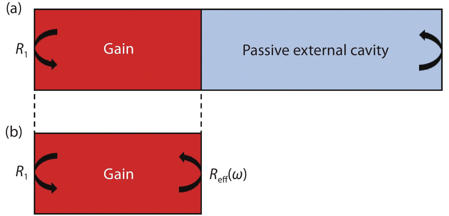
A WEC-NLSL, as is illustrated in Fig. 1(a), includes a semiconductor active section and a passive external cavity. The active section, which typically contains a III–V semiconductor quantum wells structure, is used to provide the optical gain for the whole cavity and thereby determines the lasing wavelength range. The passive external cavity is used to select the lasing wavelength and in the meantime to reduce the linewidth.
![]()
Figure 1.(Color online) External cavity feedback semiconductor laser. (a) Block diagram. (b) Equivalent model.
The linewidth, which is defined as the spectral width of a laser’s lasing mode, is affected by the noise due to the phase fluctuation in the laser output power. At the lower frequency range, the noise spectrum density, which is closely related with the measured frequency, is dominated by various 1/f noises and other types of “technical noises” that originate from external sources. At higher frequencies where 1/f noise and other technical noises become vanished, white noise caused by the random process of spontaneous emission and carrier fluctuations becomes dominant. This is irrelevant to the measured frequency and completely determined by the laser structure, which makes the main contribution to the minimum achievable linewidth of a laser. In this paper, we limit our study to the linewidth under higher frequency noise, which is also referred to as the Lorentz linewidth[
To obtain the steady-state analysis and qualitatively evaluate the linewidth of a WEC-NLSL, the entire waveguide external cavity is treated as a resonant mirror, so the equivalent cavity model of the WEC-NLSL is shown in Fig. 1(b).
According to the above equivalent model and the adiabatic chirp theory, the linewidth of a WEC-NLSL can be expressed as follows[
where Δν0 represents the Schawlow–Townes linewidth of the solitary Fabry–Pérot laser with mirror reflectivity R1 and
In Eqs. (1)–(4), factor A reflects the increase in a roundtrip accumulated phase, which is equivalent to the effective cavity length enhancement mainly provided by the external cavity. Factor B represents the magnitude of the optical negative feedback effect, which is proportional to the magnitude of αH. From the equations above, one can see that both factors A and B have a direct impact on the laser’s spectrum linewidth. An increase of the factor A means that the passive section length of the laser cavity becomes longer, leading to the increased photon lifetime. Fig. 2(a) shows the effective cavity length as a function of the optical frequency in the external cavity configuration, and one can see that only when the lasing frequency is aligned with the resonance peak frequency, both the effective cavity length and factor A is maximized. An external cavity also induces an optical negative feedback effect, which is mainly described by factor B. The optical negative feedback effect can stabilize the lasing frequency, thereby effectively reducing the linewidth, as shown in Fig. 2(b). Since factor A is maximized at the resonance frequency of the external cavity, and factor B peaks at the frequency that is slightly detuning from the external cavity resonance, the optimal point must be carefully selected to obtain the narrowest laser linewidth. Also, as the linewidth enhancement factor αH has a positive effect in factor B but a negative effect in the Schawlow–Towns linewidth, the quantum well structure should be carefully optimized as well. Furthermore, an increase in the output power P0 leads to a reduction in the linewidth, as the linewidth is inversely proportional to the laser power as shown in Eq. (4). However, the higher laser power will result in high amplified spontaneous emission noise, which further broadens the linewidth.
![]()
Figure 2.(Color online) (a) Illustration of the role of factor
As discussed above, only the loss-reduction behavior can monotonously improve the linewidth performance of the semiconductor lasers. However, the internal loss αi is difficult to reduce as the active material and structure are basically fixed. Therefore, the loss-reduction in the external cavity becomes the most effective way to achieve narrow linewidth through the increase of factor A and B, which is the reason why narrow-linewidth semiconductor lasers are usually realized by the external cavity.
3. Technologies of WEC-NLSL
3.1. Low-loss waveguide
As is discussed above, linewidth improvement can be made monotonously by employing a low-loss/long passive section external waveguide. Hence, our discussion only focuses on the external passive waveguide, from the point of both material choice and waveguide configurations.
In order for the passive waveguide to work more effectively in terms of linewidth improvement, a key requirement is that the waveguide has low loss. Thus far, silicon oxynitride (SiON), silica (SiO2), Si-wire, silicon nitride (Si3N4), and silicon-on-insulator (SOI) have been selected as waveguide external cavity platforms and kHz-scaled linewidth has been achieved. Their basic optical properties are listed in Table 1.
As shown in Table 1, the SiON and silica waveguide external cavity have low propagation loss, the WEC-NLSL with a linewidth of tens of kHz was firstly realized[
3.2. Long optical cavity length
In order to appreciate the influence of the optical length and the loss in the external cavity waveguide on the Lorentz linewidth of the lasers more clearly, Boller’s team[
![]()
Figure 3.(Color online) The relationship between the external cavity length, the waveguide loss and the intrinsic linewidth of the laser [
As shown in Fig. 3, no matter what external cavity material is selected, when the optical length is less than 1 mm, the linewidth is limited to 100 kHz. The longer the optical path of the external cavity, the more significant the impact of the waveguide loss on the linewidth. Therefore, one has to consider the feasible approach to extend the external cavity length within a small single chip. Currently, two approaches have been developed, namely micro-ring resonators (MRR) and spiral waveguides. MRR is a traveling-wave resonator, its effective optical path Leff can be expressed as the following[
where β = 2πneff/λ is the propagation constant (complex) and φ = βL is the phase change of light. L is the circumference. At the critical coupling condition, Eq. (5) becomes
where κ is the power coupling coefficient. From Eqs. (5) and (6), one can see that the effective cavity length Leff is not only determined by the physics length, but also strongly dependent on κ and propagation loss α. Fig. 4 shows the relationship between the enhancement factor (Leff/L) of the optical path and κ under different waveguide losses.
![]()
Figure 4.(Color online) Optical path extension under different coupling coefficients and different losses.
As shown in Fig. 4, in the weakly coupled low-loss MRR, the effective optical path can be significantly increased. Thus, in order to achieve a long effective optical length, the MRR circumference and κ must be appropriately designed for waveguides with different losses. Fig. 4 shows that the Leff/L of about 400 when κ of a lossless MRR is about 10% (black line). This means that an MRR with a circumference of 2.5 mm can actually be equivalent to a 1-m-long optical length in terms of the linewidth performance. At such conditions, the Lorentz linewidth of Hz level is expected, as shown in Fig. 3. Based on this simple analysis, one can see that it is possible to achieve a very narrow-linewidth performance by using a well-designed WEC-NLSL. Besides, multiple MRRs can also provide wide spectrum tuning because of the Vernier effect.
3.3. Integration technology
Although the external cavity based on the MRR configuration described above is the most effective way for reducing the linewidth, the external cavity has to be integrated with an active gain section. And this would rule out the consideration of using pure Si-based materials as they are unable to produce light efficiently. Whilst germanium lasers on silicon have been demonstrated, unfortunately, their efficiency is inadequate for most practical applications[
To date, the more commonly used integration methods are hybrid integration and heterogeneous integration. Hybrid integration refers to assembling the III–V active gain section and the external silicon photonic waveguide together by the butt-coupling technique. Although the waveguide external cavity and gain chip, which can be optimized independently, are relatively simple to fabricate in this hybrid integration, the challenge lies in the butt-coupling between the two chips. Firstly, the large coupling loss induced by the mode mismatch must be reduced as far as possible. The spot size converter (SSC), which is typically shown in Fig. 5(a), is widely employed to reduce their optical mode coupling loss. However, millimeter-level long converters are usually required for achieving small coupling loss, which is not favorable for compact narrow linewidth lasers. Secondly, the air gap between the two chips is unavoidable, thus the facet reflection is another problem, and polarization loss are also introduced, which degrade the laser linewidth. Moreover, the facets with extremely low reflectivity are difficult to implement. Both issues above will impact the laser linewidth performance.
![]()
Figure 5.(Color online) (a) SSC structure diagram[
Heterogeneous integration is a technique that directly bonds unprocessed III–V material on the top of silicon waveguides. Therefore, it is compatible with the Si CMOS process, which can effectively reduce the manufacturing cost. Compared with the hybrid integration, devices with heterogeneous integration have improved the mechanical performance, provided the bonding quality is adequate. However, the quality is actually affected by a number of factors such as bonding process, lattice mismatch, thermal expansion coefficients of the materials, and is proven to be a challenge. Currently, the main bonding methods are molecular bonding based on van der Waals force[
4. The state of art of WEC-NLSL
4.1. Butt coupling technology-based hybrid lasers
The butt coupling technology, which is relatively mature and well-developed, is very attractive because it offers one the opportunity to optimize the gain chip and external cavity separately. Several dielectric waveguide platforms, such as SiON, SiO2, Si-wire, and Si3N4, have been developed for manufacturing external cavities to form so-called hybrid integrated lasers. The main representative research institutions are the NEC Corporation of Japan, Tohoku University, Tsinghua University, the University of Twente, Clemson University, Cornell University, and the University of California, Santa Barbara (UCSB).
Fig. 6 shows the progress made in reducing the laser spectral linewidth based on the butt coupling technology under different material platforms.
![]()
Figure 6.(Color online) The intrinsic linewidth of hybrid integrated laser based on butt coupling technology: a-[
As shown in Fig. 6, early researchs about WEC-NLSLs based on SiON materials were mainly conducted by NEC, with a footprint of about 6.5 × 4.5 mm2, and a high wavelength tuning power consumption. Its linewidth is around 100 kHz[
![]()
Figure 7.(Color online) Schematic view of the hybrid laser based on a Si3N4 feedback circuit comprising a spiral and three MRRs[
Domestic researches on WEC-NLSLs started late, and only Huawei and Tsinghua University have made relevant reports[
Due to the mature and well-developed butt coupling technology, Redfern Integrated Optics (RIO)[
4.2. Heterogeneous integrated semiconductor lasers
Using heterogeneous integration technology for hybrid integration, the external cavity is manufactured only on the SOI platform. The main players include the III–V laboratory in France, the France CEA LETI, the University of Ghent in Belgium, and the UCSB in the United States. Among them, UCSB has done a lot of research and is in an international leading position.
UCSB first successfully bonded the III–V gain materials on a silicon waveguide in 2005[
![]()
Figure 8.(a) Laser structure diagram based on triple MRR. (b) Frequency noise spectrum[
The performance of heterogeneously integrated lasers produced by the Bowers’ team in recent years is shown in Table 2.
Compared with butt coupling technology, there are no commercial lasers based on heterogeneous integration technology. However, this technology is considered to be one of the most promising technologies for realizing an efficient narrow linewidth light source.
5. Summary and prospect
In summary, with the development of low-loss materials, hybrid integration and delicate designs based on the MRR unit, the intrinsic linewidth of the WEC-NLSL is gradually reduced down to the limitation. Moreover, other performances of these lasers are also enhanced rapidly. For example, by hybrid integrating a booster semiconductor optical amplifier, the laser output power reached up to 100 mW[
WEC-NLSLs have already achieved a linewidth of sub-kHz, which meets the linewidth requirements of the most coherent detection applications. However, frequency stability and mode hopping become a common problem for this kind of narrow-linewidth laser. The long external cavity length will undoubtedly reduce the mode spacing, which will result in a serious frequency noise problem and degrades the whole performance of the lasers. Thus, how to obtain a stable frequency and narrow linewidth output is one of the key issues that must be solved in the practical applications of WEC-NLSLs. The optical negative feedback method proposed by Tohoku University seems to be a way forward to realize frequency stabilization and narrow linewidth simultaneously[
Compared with the narrow linewidth semiconductor lasers with dielectric waveguide external cavity based on hybrid and heterogeneous integration technology, monolithic integration completely based on the III–V semiconductor material system is a viable approach to achieve the required spectral linewidth as well as the cost and energy consumption, as it eliminates the need for the complex hybrid integration process, the whole chip can be fabricated through the conventional III–V semiconductor batch processing, and the coupling loss between the gain section and the waveguide external cavity can be negligible. However, the intrinsic loss of III–V materials is high, which prevent them from realizing a narrow linewidth laser. Researchers are working on the optimal fabrication process and laser structure. The Eindhoven University of Technology (TU/e) in the Netherlands reduces the InP waveguide loss from 2 dB/cm to below 0.4 dB/cm via local diffusion of zinc in 2016[
Acknowledgements
This work was supported by Jiangsu Province Key R&D Program (Industry Prospect and Common Key Technologies) (No. BE2014083); Jiangxi Natural Science Foundation Project (No. 2019ACBL20054)
References
[1] X Bao, W Li, Z Qin et al. OTDR and OFDR for distributed multi-parameter sensing. Proc SPIE, 9062(2014).
[2]
[3] X Sun, J B Abshire. Comparison of IPDA lidar receiver sensitivity for coherent detection and for direct detection using sine-wave and pulsed modulation. Opt Express, 20, 21291(2012).
[4]
[5] J R Demers, R T Logan, E R Brown. An optically integrated coherent frequency-domain THz spectrometer with signal-to-noise ratio up to 80 dB. Microw Photonics, 92(2007).
[6]
[7]
[8] L Atzori, A Iera, G Morabito. The internet of things: A survey. Comput Netw, 54, 2787(2010).
[9] D Marpaung, M Burla, J Capmany. New opportunities for integrated microwave photonics. IEEE Photonics Technol Lett, 30, 1813(2018).
[10] N Dostart, B Zhang, A Khilo et al. Serpentine optical phased arrays for scalable integrated photonic LIDAR beam steering. Optica, 7, 726(2020).
[11]
[12] T Nagatsuma, H Ito, K Iwatsuki. Generation of low-phase noise and frequency-tunable millimeter-/terahertz-waves using optical heterodyning techniques with uni-traveling carrier photodiodes. 2006 European Microwave Conference, 1103(2006).
[13] V M Gelikonov. Measurement of nanoangström oscillatory displacements by a gas laser with a small natural linewidth. Radiophys Quantum Electron, 41, 998(1998).
[14] S Mo, X Huang, S Xu et al. 600-Hz linewidth short-linear-cavity fiber laser. Opt Lett, 39, 5818(2014).
[15] D Lo, S K Lam, C Ye et al. Narrow linewidth operation of solid state dye laser based on sol-gel silica. Opt Commun, 156, 316(1998).
[16] C K Laue, R Knappe, K J Boller et al. Wavelength tuning and spectral properties of distributed feedback diode lasers with a short external optical cavity. Appl Opt, 40, 3051(2001).
[17] P Signoret, M Myara, J P Tourrenc et al. Bragg section effects on linewidth and lineshape in 1.55-
[18] C H Henry. Theory of the linewidth of semiconductor lasers. IEEE J Quantum Electron, 18, 259(1982).
[19] K Y Liou, K Duttan, A Burrusc. Linewidth narrow distributed feedback injection lasers with long cavity length and detuned Bragg wavelength. Appl Phys Lett, 50, 489(1987).
[20] J Ma, L R Wang, Y T Zhao et al. Absolute frequency stabilization of a diode laser to cesium atom-molecular hyperfine transitions via modulating molecules. Appl Phys Lett, 91, 161101(2007).
[21] E Patzak, A Sugimura, S Saito et al. Semiconductor laser linewidth in optical feedback configurations. Electron Lett, 19, 1026(2007).
[22] M R Olcay, J A Pasqual, J A Lisboa et al. Tuning of a narrow linewidth pulsed dye laser with a Fabry-Perot and diffraction grating over a large wavelength range. Appl Opt, 24, 3146(1985).
[23] W Liang, V S Ilchenko, A A Savchenkov et al. Whispering-gallery-mode-resonator-based ultranarrow linewidth external-cavity semiconductor laser. Opt Lett, 35, 2822(2010).
[24]
[25] M A Tran, D Huang, J Bowers. Tutorial on narrow linewidth tunable semiconductor lasers using Si/III-V heterogeneous integration. APL Photonics, 4, 111101(2019).
[26] T Komljenovic, J E Bowers. Monolithically integrated high-
[27]
[28] H Ou. Different index contrast silica-on-silicon waveguides by PECVD. Electron Lett, 39, 212(2003).
[29] W Bogaerts, R Baets, P Dumon et al. Nanophotonic waveguides in silicon-on-insulator fabricated with CMOS technology. J Lightwave Technol, 23, 401(2005).
[30] X Ji, F A S Barbosa, S P Roberts et al. Ultra-low-loss on-chip resonators with sub-milliwatt parametric oscillation threshold. Optica, 4, 619(2017).
[31] M Tran, D Huang, T Komljenovic et al. Ultra-low-loss silicon waveguides for heterogeneously integrated silicon/III-V photonics. Appl Sci, 8, 1139(2018).
[32] T Takeuchi, M Takahashi, K Suzuki et al. Wavelength tunable laser with silica-waveguide ring resonators. IEICE Trans Electron, 92, 198(2009).
[33] A H Atabaki, E S Hosseini, A A Eftekhar et al. Optimization of metallic microheaters for high-speed reconfigurable silicon photonics. Opt Express, 18, 18312(2010).
[34] G Poberaj, H Hu et al. Lithium niobate on insulator (LNOI) for micro-photonic devices. Laser Photon Rev, 6, 488(2012).
[35] M Belt, M L Davenport, J E Bowers et al. Ultra-low-loss Ta2O5-core/SiO2-clad planar waveguides on Si substrates. Optica, 4, 532(2017).
[36] K J Boller, A V Rees, Y Fan et al. Hybrid integrated semiconductor lasers with silicon nitride feedback circuits. Photonics, 7, 4(2019).
[37] B Liu, A Shakouri, J E Bowers. Passive microring-resonator-coupled lasers. Appl Phys Lett, 79, 3561(2001).
[38] J F Liu, X C Sun, R Camacho-Aguilera et al. Ge-on-Si laser operating at room temperature. Opt Lett, 35, 679(2010).
[39] G T Reed, A P Knights, M Liao et al. Integrating III-V quantum dot lasers on silicon substrates for silicon photonics. SPIE Opto, 101081A(2017).
[40]
[41] G Roelkens, L Liu, D Liang et al. III-V/silicon photonics for on-chip and intra-chip optical interconnects. Laser Photon Rev, 4, 751(2010).
[42] T Tsuchizawa, K Yamada, H Fukuda et al. Microphotonics devices based on silicon microfabrication technology. IEEE J Sel Top Quantum Electron, 11, 232(2005).
[43]
[44] K Suzuki, J A Kubby, G T Reed et al. Wavelength tunable laser diodes with Si-wire waveguide ring resonator wavelength filters. Proc SPIE, 7943, 79431G(2011).
[45] K Nemoto, T Kita, H Yamada. Narrow-spectral-linewidth wavelength-tunable laser diode with Si wire waveguide ring resonators. Appl Phys Express, 5, 2701(2012).
[46] R M Oldenbeuving, E J Klein, H L Offerhaus et al. 25 kHz narrow spectral bandwidth of a wavelength tunable diode laser with a short waveguide-based external cavity. Laser Phys Lett, 10, 015804(2013).
[47]
[48] T Kita, K Nemoto, H Yamada. Silicon photonic wavelength-tunable laser diode with asymmetric Mach-Zehnder interferometer. IEEE J Sel Top Quantum Electron, 20, 344(2014).
[49] T Kita, K Nemoto, H Yamada. Long external cavity Si photonic wavelength tunable laser diode. Jpn J Appl Phys, 53, 04E(2014).
[50]
[51]
[52] N Kobayashi, K Sato, M Namiwaka et al. Silicon photonic hybrid ring-filter external cavity wavelength tunable lasers. J Lightwave Technol, 33, 1241(2015).
[53] R Tang, T Kita, H Yamada. Narrow-spectral-linewidth silicon photonic wavelength-tunable laser with highly asymmetric Mach-Zehnder interferometer. Opt Lett, 40, 1504(2015).
[54]
[55]
[56] T Kita, R Tang, H Yamada. Narrow spectral linewidth silicon photonic wavelength tunable laser diode for digital coherent communication system. IEEE J Sel Top Quantum Electron, 22, 23(2016).
[57] S Brian, J Xingchen, D Avik et al. Compact narrow-linewidth integrated laser based on a low-loss silicon nitride ring resonator. Opt Lett, 42, 4541(2017).
[58]
[59] Y Lin, C Browning, R B Timens et al. Characterization of hybrid InP-TriPleX photonic integrated tunable lasers based on silicon nitride (Si3N4/SiO2) microring resonators for optical coherent system. IEEE Photonics J, 10, 1(2018).
[60] Y Li, Y Zhang, H Chen et al. Tunable self-injected fabry-perot laser diode coupled to an external high-
[61] Y Zhu, L Zhu. Narrow-linewidth, tunable external cavity dual-band diode lasers through InP/GaAs-Si3N4 hybrid integration. Opt Express, 27, 2354(2019).
[62] C Xiang, P A Morton, J E Bowers. Ultra-narrow linewidth laser based on a semiconductor gain chip and extended Si3N4 Bragg grating. Opt Lett, 44, 3825(2019).
[63] Y Y Zhu, S W Zeng, L Zhu. Optical beam steering by using tunable, narrow-linewidth butt-coupled hybrid lasers in a silicon nitride photonics platform. Photonics Res, 8, 03000375(2020).
[64] Y W Fan, A van Rees, P J Van der Slot et al. Hybrid integrated InP-Si3N4 diode laser with a 40-Hz intrinsic linewidth. Opt Express, 28, 21713(2020).
[65] Y Hu, W Cao, X S Tang et al. High power, high SMSR and wide tuning range silicon micro-ring tunable laser. Opt Express, 25, 8029(2017).
[66]
[67] H Park, A W Fang, S Kodama et al. Hybrid silicon evanescent laser fabricated with a silicon waveguide and III-V offset quantum wells. Opt Express, 13, 9460(2005).
[68]
[69] S Keyvaninia, G Roelkens, D Van Thourhout et al. Demonstration of a heterogeneously integrated III-V/SOI single wavelength tunable laser. Opt Express, 21, 3784(2013).
[70] J C Hulme, J K Doylend, J E Bowers. Widely tunable Vernier ring laser on hybrid silicon. Opt Express, 21, 19718(2013).
[71] T Komljenovic, S Srinivasan, E Norberg et al. Widely tunable narrow-linewidth monolithically integrated external-cavity semiconductor lasers. IEEE J Sel Top Quantum Electron, 21, 214(2015).
[72]
[73]
[74]
[75] D Huang, M A Tran, J Guo et al. High-power sub-kHz linewidth lasers fully integrated on silicon. Optica, 6, 745(2019).
[76] M A Tran, D Huang, J Guo et al. Ring-resonator based widely-tunable narrow-linewidth Si/InP integrated lasers. IEEE J Sel Top Quantum Electron, 26, 1(2019).
[77] K Aoyama, S Kobayashi, M Wada et al. Compact narrow-linewidth optical negative feedback laser with Si optical filter. Appl Phys Express, 11, 112703(2018).
[78] G D’Agostino et al. Low-loss passive waveguides in a generic InP foundry process via local diffusion of zinc. Opt Express, 23, 25143(2015).
[79] S Andreou, K A Williams, E A J M Bente. Monolithically integrated InP-based DBR lasers with an intra-cavity ring resonator. Opt Express, 27, 26281(2019).
[80] J Wang, R Y Zhan, B C Qiu et al. Design of high-
[81] C C Luo, J Wang, B C Qiu et al. Gain spectral narrowing of semiconductor laser based on dual-core vertical coupler structure. Opt Commun, 474, 126166(2020).
[82]
[83]


Set citation alerts for the article
Please enter your email address

© Copyright 2018-2021 | Chinese Laser Press. All Rights Reserved 沪ICP备15018463号-20