
Shagun Pal, Brijesh Kumar. Mathematical analysis of organic-pass transistor using pseudo-p-OTFTs[J]. Journal of Semiconductors, 2020, 41(6): 062601
- Journal of Semiconductors
- Vol. 41, Issue 6, 062601 (2020)
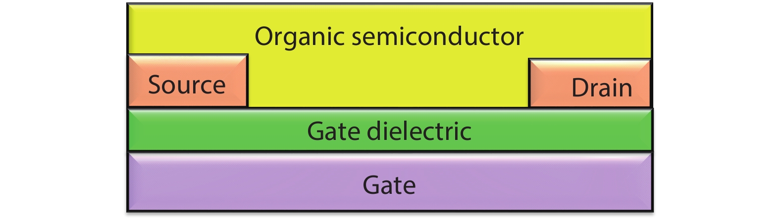
Fig. 1. (Color online) Schematic representation of the bottom gate bottom contact organic thin film transistor.
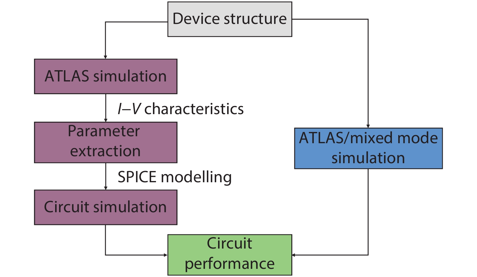
Fig. 2. (Color online) Schematic representation of the mixed mode analysis of ATLAS for circuit implementation.
Fig. 3. (Color online) Experimental[9 ] and simulated device results: (a) output and (b) transfer characteristics curve.
Fig. 4. (Color online) Transfer characteristics curve validity of simulated device through model[21 ] and experimental[9 ].
Fig. 5. (Color online) (a) The basic circuitry for logic high organic-PT. (b) Variation of output voltage with respect to time through MATLAB. (c) Simulation result for the logic high signal with the input supply of 5 V.
Fig. 6. (Color online) (a) The basic circuitry for logic low organic-PT. (b) working principle of the proposed model for logic low signal. (c) Variation of output voltage with respect to time through MAT Lab. (d) Simulation result for the logic low signal with the input supply of 5 V.
|
Table 1. Device parameters for the organic material based device[9 ].
|
Table 2. Electrical parameter comparison of pentacene-based single gate organic thin film transistor.
|
Table 3. Fitting parameters for the transfer characteristics using the model through MATLAB[21 ].
|
Table 4. Comparison between analytical and simulation parameters for logic high transfer signal.
|
Table 5. Dimensions for the simulated parameters of the proposed inverter design.
|
Table 6. Comparison between analytical and simulation parameters for logic low transfer signal.

Set citation alerts for the article
Please enter your email address
© Copyright 2018-2021 | Chinese Laser Press. All Rights Reserved 沪ICP备15018463号-20